Vacuum circuit chip packaging mould

A circuit chip and vacuum technology, applied in the manufacture of circuits, electrical components, semiconductor/solid-state devices, etc., can solve the problems of poor exhaust effect, easy residual bubbles, no degassing device, etc., to achieve smooth surface, fast installation speed, Good degassing effect

Inactive Publication Date: 2019-06-04
湖南正美光电科技有限公司
View PDF0 Cites 3 Cited by
  • Summary
  • Abstract
  • Description
  • Claims
  • Application Information

AI Technical Summary

Problems solved by technology

Existing electronic packaging molds generally have an upper mold and a lower mold that are used in conjunction with each other, and since the contact surfaces of the upper mold and the lower mold are relatively smooth planes, it is difficult to control the installation position of the upper mold and the lower mold when they are installed. , repeated adjustments are required to achieve precise installation of the upper and lower dies
[0003] In addition, the existing electronic packaging molds generally do not have a degassing device. Even if a few packaging molds have a degassing function, they generally rely on the flow of

Method used


Image

  • Vacuum circuit chip packaging mould
  • Vacuum circuit chip packaging mould
  • Vacuum circuit chip packaging mould

Examples


Embodiment Construction

[0017] The present invention will be further described below in conjunction with the accompanying drawings.

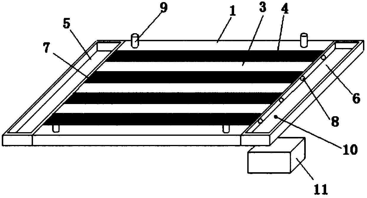
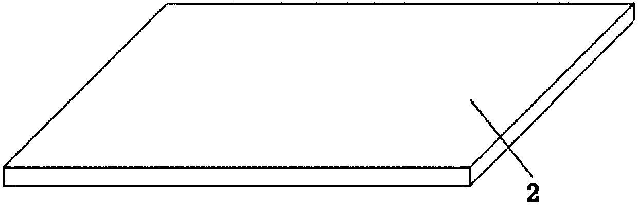
[0018] Such as Figure 1~2 As shown, the vacuum circuit chip packaging mold is characterized in that it includes: a lower mold 1 and an upper mold 2, and the lower mold 1 includes a plurality of parallel platforms 3 arranged at intervals and cavities 4 for placing electronic components. The two ends of the platform 3 and the cavity 4 are respectively provided with a feeding trough 5 and a surplus material discharge chute 6, and the connecting end between the cavity 4 and the feeding trough 5 is provided with a feed hole 7, and the cavity 4 is provided with a discharge hole 8 at the connection end of the residual material discharge tank 6; a vacuum hole 10 is provided at the bottom of the residual material discharge tank 6, and the vacuum hole 10 is connected with a vacuum pump 11.

[0019] The platform 3 is provided with a plurality of positioning columns 9 , and the ...


PUM


Abstract

The invention discloses a vacuum circuit chip packaging mould. The vacuum circuit chip packaging mould is characterized in that the vacuum circuit chip packaging mould comprises a lower mould(1) and an upper mould (2), the lower mould (1) comprises a plurality of platforms (3) and a mold cavity (4), wherein the platforms are horizontally arranged at intervals, the mold cavity (4) is used for placing electron components, feeding grooves (5) and residual material discharging grooves (6) are correspondingly formed in the two ends of the platforms (3) and the mold cavity (4), feeding holes (7) areformed in the connecting ends of the mold cavity (4) and the feeding grooves (5), and discharging holes (8) are formed in the connecting ends of the mold cavity (4) and the residual material discharging grooves (6); and vacuum holes (10) are formed in the bottom ends of the residual material discharging grooves (6), and the vacuum holes (10) are connected with a vacuum pump (11). According to thevacuum circuit chip packaging mould, the degassing effect is great, and the vacuum circuit chip packaging mould is particularly suitable for degassing and packaging of packaging materials with largestickiness and bad mobility.

Description

technical field [0001] The invention relates to a vacuum circuit chip packaging mold, which belongs to the technical field of circuit chip packaging. Background technique [0002] Circuit chip packaging is to install the integrated circuit built-in chip for external use, which plays a role in placing, fixing and sealing, protecting the integrated circuit built-in chip, and enhancing the ability to adapt to the environment. Existing electronic packaging molds generally have an upper mold and a lower mold that are used in conjunction with each other, and since the contact surfaces of the upper mold and the lower mold are relatively smooth planes, it is difficult to control the installation position of the upper mold and the lower mold when they are installed. , repeated adjustments are required to achieve precise installation of the upper and lower dies. [0003] In addition, the existing electronic packaging molds generally do not have a degassing device. Even if a few packa...

Claims


Application Information

Patent Timeline
IPC IPC(8): B29C39/26B29C39/42B29C39/10B29C33/30H01L21/56
Inventor 刘汉平刘林峰刘燕米玖帆
Owner 湖南正美光电科技有限公司
Why Eureka
Try Eureka