A micro-semiconductor nozzle structure

A semiconductor and miniature technology, which is applied in the direction of machines/engines, jet propulsion devices, gas turbine devices, etc., can solve the problems of short service life of micro-semiconductor electric nozzles, scrapping of micro-semiconductor electric nozzles, and high discharge voltage under air pressure, so as to avoid product scrapping , Improve the appearance of welding and the effect of improving product performance

Active Publication Date: 2021-12-24
SHAANXI AVIATION ELECTRICAL
View PDF9 Cites 0 Cited by
  • Summary
  • Abstract
  • Description
  • Claims
  • Application Information

AI Technical Summary

Problems solved by technology

[0005] The biggest defect of the current micro-semiconductor nozzle is high discharge voltage under air pressure, low pass rate, and short service life
The root cause is the linear structure of the center electrode discharge end. The design defect caused by this structure is the unavoidable gap between the center electrode 3 and the insulator 2. Under a certain air pressure, the gap will form an insulating dielectric layer that is difficult to break down , resulting in high discharge voltage under air pressure; at the same time, the linear structure of the center electrode 3 causes the size of the discharge end to be small, and the electric corrosion resistance time of the discharge end of the center electrode 3 is short during the operation of the miniature semiconductor nozzle, resulting in the service life of the miniature semiconductor nozzle short
At the same time, after brazing, due to the excessive infiltration of solder onto the thread of the housing 1 and partial thread deformation, the micro semiconductor electric nozzle is scrapped, and the product qualification rate is low.

Method used


Image

  • A micro-semiconductor nozzle structure
  • A micro-semiconductor nozzle structure
  • A micro-semiconductor nozzle structure

Examples


Embodiment Construction

[0043] Embodiments of the present invention are described in detail below, and the embodiments are exemplary and intended to explain the present invention, but should not be construed as limiting the present invention.

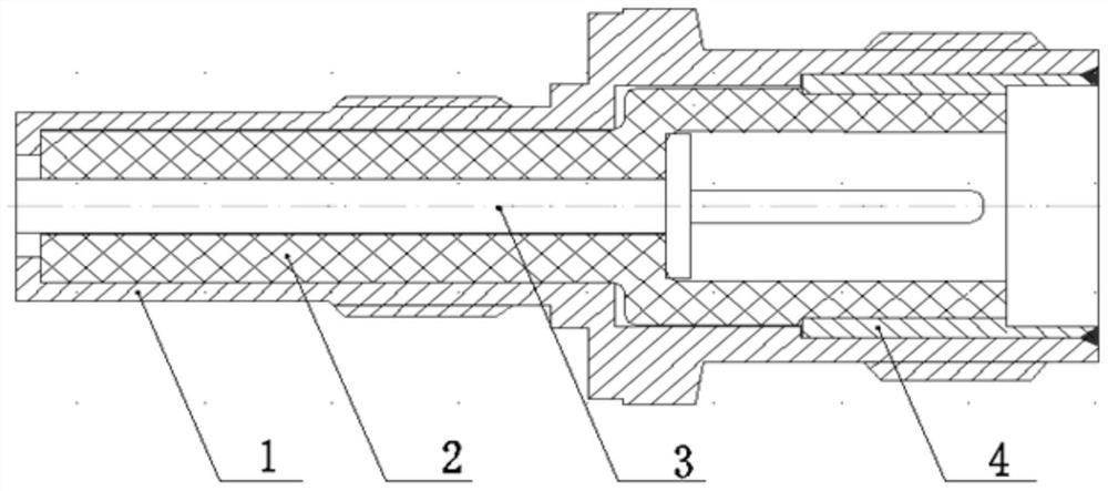
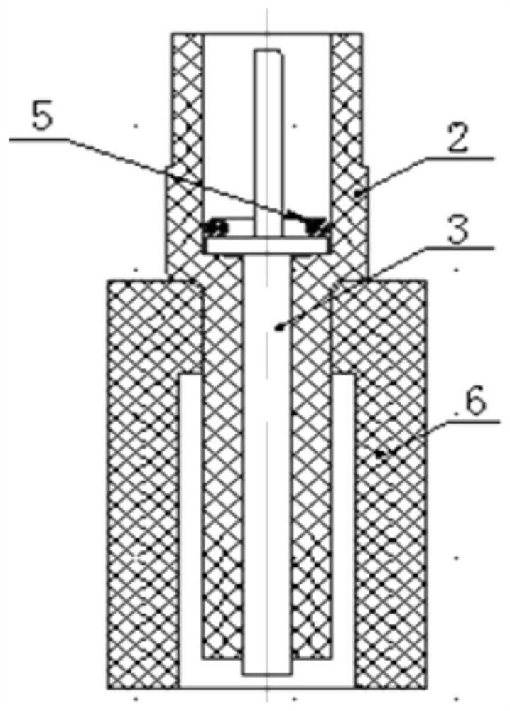
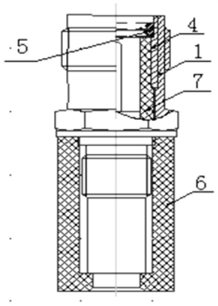
[0044] A kind of micro-semiconductor nozzle structure of the present invention, is by the parts such as housing 1, insulator 2, the center electrode 3 of discharge end band cap, sealing and fixed center electrode 3 and disc 8 of insulator 2 by means of certain tooling ( 6-1, 6-2, 6-3) are brazed in a hydrogen furnace, such as Figure 4 and Figure 5 as shown, Figure 4 Structural diagram of the miniature semiconductor electric nozzle proposed for the present invention; Figure 5 It is the brazing assembly diagram of the miniature semiconductor electric nozzle proposed by the present invention.

[0045] The electric nozzle produced by the micro-semiconductor electric nozzle structure provided by the present invention has good comprehensive performance, low d...


PUM

PropertyMeasurementUnit
diameteraaaaaaaaaa
lengthaaaaaaaaaa

Abstract

The present invention proposes a micro-semiconductor nozzle structure, including a shell, an insulator, a central electrode and a wafer. The main body of the central electrode is a stepped cylindrical structure, the discharge end has a cap, and the surface is plated with nickel; the main body of the insulator is an outer circle with a stepped surface There is a cylindrical structure with axially stepped through holes inside; the small diameter end of the insulator is the discharge end, sintered with semiconductor materials; the stepped surface of the insulator through hole and the outer circle at the same radial position as the stepped surface of the through hole have a metallization layer, and the insulator The diameter of the small-diameter section of the through hole is consistent with the diameter and length of the large-diameter section of the center electrode; there is a tool relief groove at the part corresponding to the metallization position of the outer circle of the shell and the insulator; the disc has a central through hole, and the center electrode and the insulator can be brazed through the disc. welded together. The invention reduces the discharge voltage under the air pressure of the micro-semiconductor electric nozzle, improves the qualified rate of the product, improves the product quality and prolongs its service life.

Description

technical field [0001] The invention belongs to the micro-semiconductor electric nozzle of an aero-engine, and relates to a structure of a micro-semiconductor electric nozzle. Background technique [0002] The miniature semiconductor nozzle is an important accessory of the aircraft engine. The advantages of the miniature semiconductor nozzle are simple structure and good processability; the disadvantages are high discharge voltage under air pressure, low product qualification rate and short service life. The structure of the micro-semiconductor nozzle is composed of a housing 1, an insulator 2, a center electrode 3, and a bushing 4 (see the structure diagram of the current micro-semiconductor nozzle. figure 1 ). The reason for the high discharge voltage under air pressure is that there is an unavoidable gap between the center electrode 3 and the insulator 2 (mainly because the center electrode 3 is a metal part and the insulator 2 is a ceramic part. If there is no gap betwe...

Claims


Application Information

Patent Timeline
Patent Type & Authority Patents(China)
IPC IPC(8): F02C7/266
Inventor 万思明乌凯
Owner SHAANXI AVIATION ELECTRICAL
Why Eureka
Try Eureka