Supercharge Your Innovation With Domain-Expert AI Agents!

A silicon wafer edge polishing process

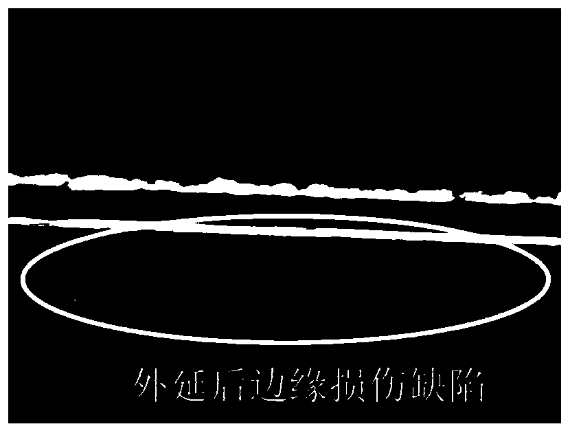
A silicon wafer and edge technology, which is applied in the field of silicon wafer edge polishing technology, can solve problems such as corrosion damage on the reference surface of silicon wafers, and achieve the effect of solving corrosion damage and improving device processing yield

Active Publication Date: 2020-04-17
山东有研半导体材料有限公司
View PDF6 Cites 0 Cited by
  • Summary
  • Abstract
  • Description
  • Claims
  • Application Information

AI Technical Summary

Problems solved by technology

[0004] The purpose of the present invention is to provide a silicon wafer edge polishing process to solve the technical problem of corrosion damage to the silicon wafer reference surface during the round edge edge polishing process in the prior art, and to improve the yield of epitaxial processing and device processing

Method used


Image

  • A silicon wafer edge polishing process
  • A silicon wafer edge polishing process
  • A silicon wafer edge polishing process

Examples


Embodiment

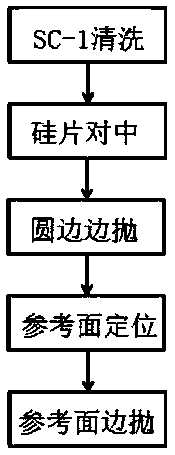
[0026] Processing of 8-inch silicon wafers with heavy As doping and a 22-degree chamfer angle

[0027] (1) Use a cleaning machine to clean the silicon wafers to be edge-thinned, and first clean them with SC-1. The SC-1 cleaning solution is composed of ammonia water, hydrogen peroxide and pure water in a ratio of 1:1:15. The cleaning time was 7 minutes, and the cleaning temperature was 70° C., and then the QDR was rinsed 3 times in a pure water tank. Finally, use the spin drying method to dry.

[0028] (2) Put the silicon wafer cleaned in step (1) into the loading table of the side throwing machine, and transport it to the centering machine by the robot for centering and positioning, ensuring that the deviation between the center of the silicon wafer and the center of the machine is within 0.2mm.

[0029] (3) Step (2) is completed to carry out round edge polishing process on the silicon wafer in the middle, the polishing cloth hardness used is 60Aske-C, and the edge polishing ...


PUM


Abstract

The invention discloses a silicon wafer edge polishing process which comprises the following steps that (1) silicon wafers are cleaned by using a cleaning machine; (2) the cleaned silicon wafers are centered on a machine table; (3) the edges of the round edges of the silicon wafers are polished; (4) reference surface positioning treatment is carried out on the silicon wafers of which polishing ofthe edges of the round edges is finished; and (5) the edges of the reference surfaces of the silicon wafers are polished after the positions of the reference surfaces are determined. The silicon waferedge polishing process effectively solves the problem of reference surface edge corrosion damage caused in the edge polishing process by increasing the cleaning treatment before edge polishing and changing the edge polishing flow sequence, smooth and undamaged reference surface edges are obtained, and the yields of epitaxial processing and device processing are improved.

Description

technical field [0001] The invention relates to a silicon wafer edge polishing process, which belongs to the technical field of silicon wafer processing. Background technique [0002] With the rapid development of the semiconductor industry along Moore's Law, the feature size of microelectronic devices is continuously shrinking, and more and more stringent requirements are put forward for the integrity, uniformity, surface quality, edge quality, and performance testing and evaluation of silicon materials. In order to improve the productivity of epitaxial wafer or device manufacturers, more stringent requirements are put forward for the edge quality of silicon wafers. For silicon wafers of 8 inches or larger, edge polishing is generally required prior to the surface polishing process. Edge polishing adopts chemical mechanical polishing. There is a thin layer of polishing liquid between the edge surface of the silicon wafer and the polishing cloth, which corrodes the edge sur...

Claims


Application Information

Patent Timeline
Patent Type & Authority Patents(China)
IPC IPC(8): B24B29/02C11D7/04C11D7/18
Inventor 路一辰王新李俊峰潘紫龙王玥李耀东曲翔史训达
Owner 山东有研半导体材料有限公司
Features
  • R&D
  • Intellectual Property
  • Life Sciences
  • Materials
  • Tech Scout
  • Unparalleled Data Quality
  • Higher Quality Content
  • 60% Fewer Hallucinations
Learn More