Simulation method for manufacturing three-dimensional atom probe sample process by FIB based on MATLAB

An atom probe and process simulation technology, applied in scanning probe technology, instruments, etc., can solve the problems of complex FIB processing process, sample preparation in indeterminate area, separation of sample and base, etc., to improve the purpose and success rate, The effect of complete programming visualization function and efficient numerical calculation function

Active Publication Date: 2019-06-18
NANJING UNIV OF SCI & TECH
View PDF10 Cites 9 Cited by
  • Summary
  • Abstract
  • Description
  • Claims
  • Application Information

AI Technical Summary

Problems solved by technology

However, this method can only be applied to metal samples, and it cannot be used for regional sample preparation for samples with specific microstructures (such as grain boundaries, phase boundaries, cracks, etc.)
The second is FIB, which can accurately prepare samples for three-dimensional atom probes and solve the problems of electrochemical polishing. However, this method also has many difficulties in the actual operation process. Rotation and tilting, it is not easy to estimate the spatial position change of the target microstructure, it is difficult to ensure that the target microstructure remains in the final APT tip sample, or to control its orientation in the final APT tip sample
In addition, the sample needs to be transferred during the FIB sample preparation process. Improper cutting angle design will increase the probability of desoldering or defects when welding Pt during the transfer process, resulting in the separation of the sample from the base or rapid fracture in the APT experiment.
[0004] In short, the FIB processing process is complicated and difficult, and it takes a long time to prepare samples, and the equipment is expensive and the cost is high.

Method used


Image

  • Simulation method for manufacturing three-dimensional atom probe sample process by FIB based on MATLAB
  • Simulation method for manufacturing three-dimensional atom probe sample process by FIB based on MATLAB
  • Simulation method for manufacturing three-dimensional atom probe sample process by FIB based on MATLAB

Examples


Embodiment Construction

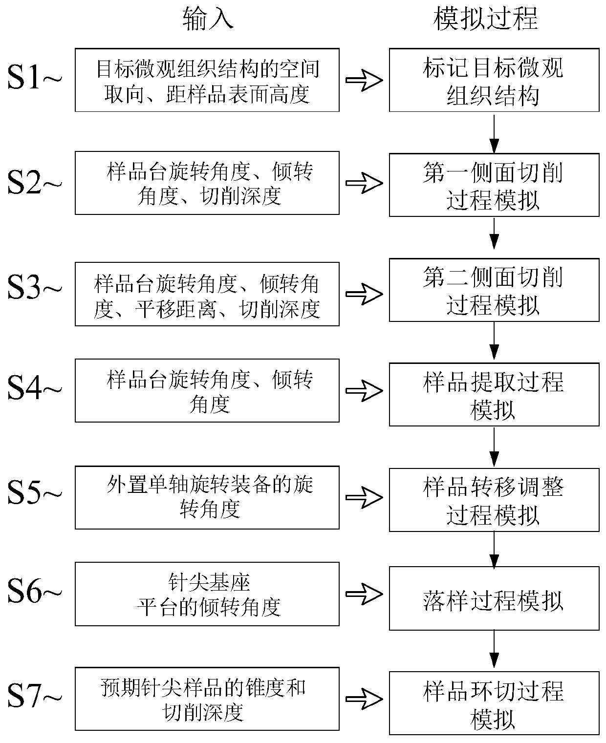
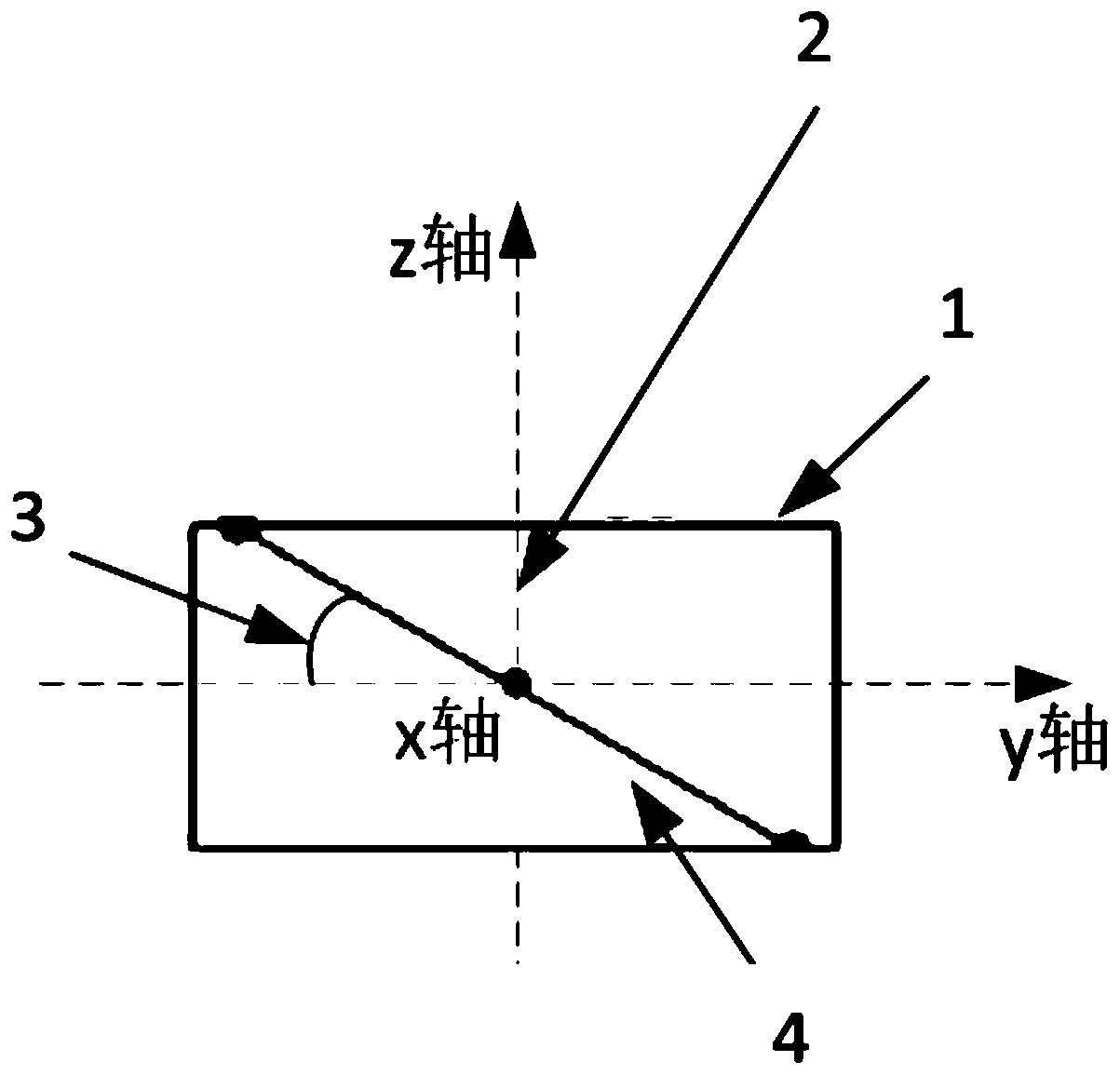
[0032] like figure 1 As shown, a MATLAB-based FIB simulation method for preparing an APT sample process includes the following steps, S1, first marking the spatial position of the target microstructure in the material to be tested. Since the microstructure of the sample surface is obtained by SEM, EBSD and other characterization means, therefore, as figure 2 As shown, the spatial position information of the target microstructure is the distance 2 between the target microstructure and the sample surface, the orientation angle 3 of the target microstructure, and the trace 4 of the target microstructure on the end surface.

[0033] S2, by setting the rotation angle R of the sample stage 1 , tilt angle T 1 and depth of cut H 1 , to simulate the first side cutting process. The rotation angle R of the sample stage 1, tilt angle T 1 Based on the angle range that can be realized by the current mainstream FIB / SEM equipment; and the cutting depth H 1 Determined according to the ...


PUM


Abstract

The invention belongs to the FIB processing field and especially relates to a simulation method of carrying out three-dimensional atom probe sample processing process by using an FIB based on MATLAB.The method comprises the following steps of S1, position marking; S2, first side surface cutting simulation: carrying out first side surface cutting process simulation by setting a sample stage rotation angle R1, a tilt angle T1, and a cutting depth H1; S3, second side surface cutting simulation: carrying out second side surface cutting process simulation as the above step; S4, sample extraction simulation: carrying out sample extraction process simulation by setting a rotation angle R3 of a sample stage and a tilt angle T3; S5, sample transfer simulation; S6, fall sample simulation; and S7, ring cutting simulation. A spatial position of a target microstructure in a detected material is marked through an MATLAB program, and rotation, tilting, translation and other motions of the sample stage during an FIB processing process are simulated so as to realize process simulation for the FIB to process an APT sample and a FIB processing parameter optimization design, and improve a purpose anda success rate of FIB processing.

Description

technical field [0001] The invention belongs to the field of FIB processing, in particular to a MATLAB-based simulation method for processing a three-dimensional atom probe (APT) sample by using a focused ion beam (FIB). Background technique [0002] APT can quantitatively give the distribution information of different element atoms in the material in three-dimensional space, making it play an important role in material science research. [0003] The samples used in the APT experiment are needle-shaped, and there are two main methods of preparation. The first is electrochemical polishing, that is, one end of a filament or thin strip sample is polished to a needle-like shape through an electrolyte, and the diameter of the top is less than 200 nanometers. However, this method can only be applied to metal samples, and cannot be used for regional sample preparation of samples with specific microstructures (such as grain boundaries, phase boundaries, cracks, etc.). The second is...

Claims


Application Information

Patent Timeline
Patent Type & Authority Applications(China)
IPC IPC(8): G01Q30/20
Inventor 靳慎豹吴修婷陈雪涵刘畅胡蓉沙刚
Owner NANJING UNIV OF SCI & TECH
Why Eureka
Try Eureka