A method of manufacturing a circuit board for realizing high-density interconnection

A manufacturing method and circuit board technology, which are applied in the directions of printed circuit components, electrical connection printed components, and electrical connection formation of printed components, can solve the problems of complex process and high manufacturing cost, achieve simple process flow, reduce manufacturing difficulty and manufacturing. cost effect

Active Publication Date: 2021-03-12
SHENZHEN SUNTAK MULTILAYER PCB
View PDF6 Cites 0 Cited by
  • Summary
  • Abstract
  • Description
  • Claims
  • Application Information

AI Technical Summary

Problems solved by technology

[0004] The present invention aims at the problem that the existing high-density interconnection circuit board adopts the microhole technology to realize the interlayer electrical connection, which requires multiple laser drilling, hole filling, electroplating and pressing processes, the process is complicated and the manufacturing cost is high. A method for making a circuit board capable of achieving high-density interconnection without using microvia technology by realizing the electrical connection function of multiple microvias in one mechanical through hole

Method used


Image

  • A method of manufacturing a circuit board for realizing high-density interconnection
  • A method of manufacturing a circuit board for realizing high-density interconnection
  • A method of manufacturing a circuit board for realizing high-density interconnection

Examples


Embodiment

[0025] This embodiment provides a method for fabricating a circuit board for high-density interconnection, which includes a method for fabricating metallized sub-holes on the circuit board, including the following steps:

[0026] (1) Cutting: cut out the inner core board according to the panel size required by the design.

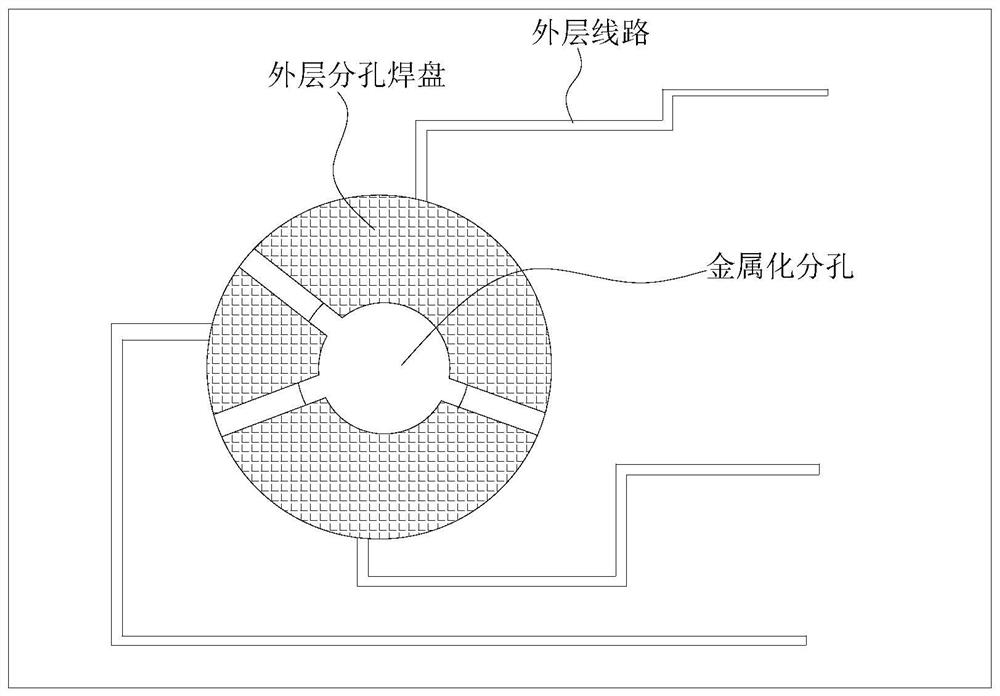
[0027] (2) Making the inner layer circuit: using the negative process to make the inner layer circuit on the inner layer core board to obtain the inner layer circuit board. The inner layer circuit includes an inner layer sub-hole pad for connection with the metallized vias that will be formed later. The inner layer sub-hole pad is composed of alternately spaced copper layers and substrate layers along the circumference, and the inner layer sub-holes The alternate arrangement of the copper layer and the substrate layer on the pad is the same as the setting of the outer layer sub-hole pad to be produced later. The copper layers of the layers are connected in...


PUM

PropertyMeasurementUnit
thicknessaaaaaaaaaa
thicknessaaaaaaaaaa

Abstract

The invention relates to the technical field of printed circuit boards, in particular to a method for manufacturing a circuit board realizing high-density interconnection. In the present invention, after pattern electroplating copper layer and tin layer, through partial tin removal and alkaline etching by laser, metallized sub-holes are formed by stripping tin, and the copper layer in the hole wall is separated by the substrate layer to form mutually independent parts, which can realize different networks The interlayer interconnection of multiple micro-holes is realized in a metallized sub-hole made by a mechanical through hole, and high-density interconnection can be realized without using micro-hole technology. Therefore, the present invention provides a high-density interconnection circuit board that realizes interlayer high-density interconnection by metallized sub-holes, and a high-density interconnection circuit board that can be produced by mechanical through-hole technology without using micro-hole technology. The manufacturing method; and because the through-hole technology is adopted, multiple laser drilling, hole-filling, electroplating and pressing are not required, and the process flow is relatively simple, which greatly reduces the manufacturing difficulty and manufacturing cost.

Description

technical field [0001] The invention relates to the technical field of printed circuit boards, in particular to a method for manufacturing a circuit board realizing high-density interconnection. Background technique [0002] With the continuous improvement of the integration of electronic systems, circuit boards are becoming more and more miniaturized, thinner and integrated, so it is inevitable that the design density of circuit boards will become higher and higher, and the application of high-density interconnection circuit boards will become more and more Many, such as mobile phones of consumer electronics. As the size of the mobile phone battery is increasing, the space for increasing the mobile phone circuit board is very small, but the performance of the mobile phone needs to be improved to meet the increasingly multi-functional and high-speed development. Therefore, when designing the circuit board, increase the number of layers and reduce the Line width, line spacin...

Claims


Application Information

Patent Timeline
Patent Type & Authority Patents(China)
IPC IPC(8): H05K1/11H05K3/42
Inventor 袁为群杨辉腾罗练军孙保玉
Owner SHENZHEN SUNTAK MULTILAYER PCB
Why Eureka
Try Eureka