Packaging structure and forming method thereof

A technology of packaging structure and sealing ring, which is applied in the direction of electrical components, electric solid devices, circuits, etc., can solve the problems of packaging structure performance deterioration and achieve the effects of improving performance, reducing exposure, and improving cracking

Active Publication Date: 2019-06-21
SEMICON MFG INT (SHANGHAI) CORP +1
View PDF5 Cites 2 Cited by
  • Summary
  • Abstract
  • Description
  • Claims
  • Application Information

AI Technical Summary

Problems solved by technology

[0004] However, the performance of the packaging structure obtained by using the above-mentioned packaging technology needs to be improved, especially after t

Method used


Image

  • Packaging structure and forming method thereof
  • Packaging structure and forming method thereof
  • Packaging structure and forming method thereof

Examples


Embodiment Construction

[0043] It can be seen from the background art that the performance of the packaging structure obtained in the prior art needs to be improved.

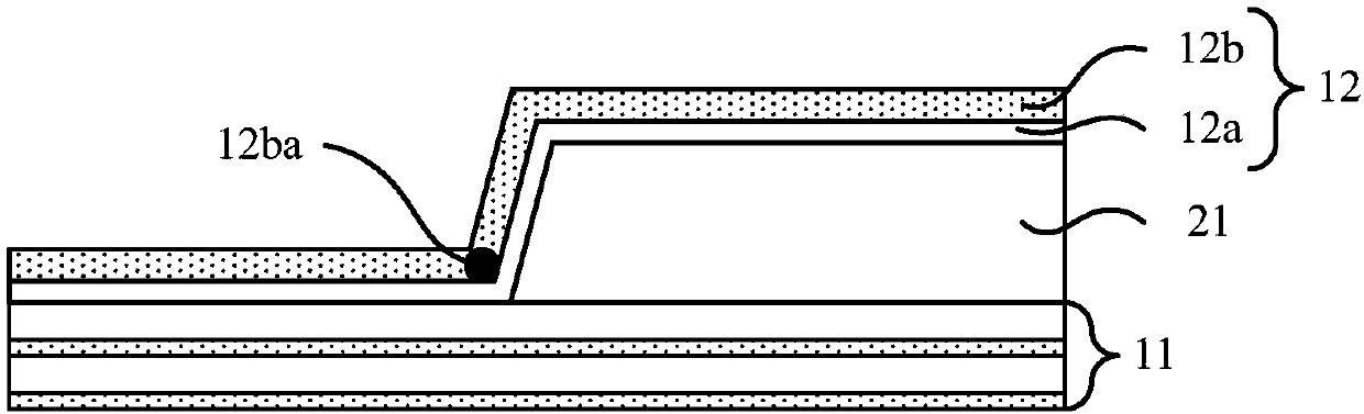
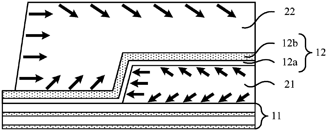
[0044]After performing PFA (Physical Failure Analysis) analysis on the package structure, it was found that cracks appeared in the passivation layers (passivation layers) near the step corner area of ​​the first wiring layer, so that the first wiring layer in the step corner area A wiring layer is exposed. The exposed first wiring layer is easily corroded, resulting in poor performance or even failure of the packaging structure.

[0045] The reasons for the cracks in the passivation layer are analyzed in combination with a method of forming a packaging structure:

[0046] refer to Figure 1 to Figure 3 , shows a schematic diagram of cross-sectional results corresponding to each step of a packaging structure forming method.

[0047] Such as figure 1 As shown, a substrate is provided with a lower passivation layer 11 on the substrate...


PUM

PropertyMeasurementUnit
Thicknessaaaaaaaaaa
Widthaaaaaaaaaa

Abstract

The invention discloses a packaging structure and a forming method thereof. The packaging structure comprises a wafer which comprises a chip region and a peripheral region which surrounds the chip region; a first wiring layer distributed on the wafer of the chip region in a discrete manner; an upper passivation layer covering the top and the side wall of the first wiring layer and extending to thewafer; and an isolation layer located on the upper passivation layer, arranged on the chip region and extending to a part of the peripheral region, wherein an isolation groove surrounding the chip region is formed in the isolation layer on the peripheral region, and the isolation groove penetrates through a part of the thickness of the isolation layer. The isolation groove can block the conduction of the internal stress action of the isolation layer to realize the release of the internal stress action of the isolation layer, thereby reducing the cracking probability of the upper passivation layer, reducing the occurrence of the exposure phenomenon of the first wiring layer, and improving the performance of the packaging structure.

Description

technical field [0001] The invention relates to the technical field of semiconductor manufacturing, in particular to a packaging structure and a forming method thereof. Background technique [0002] Wafer level BGA (Wafer Lever BGA, WLBGA) packaging is based on BGA (Ball Grid Array) technology, which is an improved and enhanced CSP packaging technology. Wafer-level BGA technology takes the wafer as the processing object. Multiple chips are packaged, aged and tested on the wafer at the same time, and then the wafer is cut to form a single device, which can be directly mounted on the substrate or printed circuit board. . [0003] Wafer-level BGA technology has the advantages of small package size and wide support for bonding requirements, which makes the application of wafer-level BGA technology more and more widely, and the demand for products packaged with wafer-level BGA technology is also increasing. [0004] However, the performance of the packaging structure obtained b...

Claims


Application Information

Patent Timeline
IPC IPC(8): H01L23/498H01L23/00H01L21/48H01L21/762
Inventor 殷原梓
Owner SEMICON MFG INT (SHANGHAI) CORP
Why Eureka
Try Eureka