Color photovoltaic module, and preparation method and application thereof
A color photovoltaic and component technology, applied in photovoltaic power generation, electrical components, semiconductor devices, etc., can solve the problems of single color and no color during the day, and achieve the effect of improving weather resistance
- Summary
- Abstract
- Description
- Claims
- Application Information
AI Technical Summary
Problems solved by technology
Method used
Image
Examples
preparation example Construction
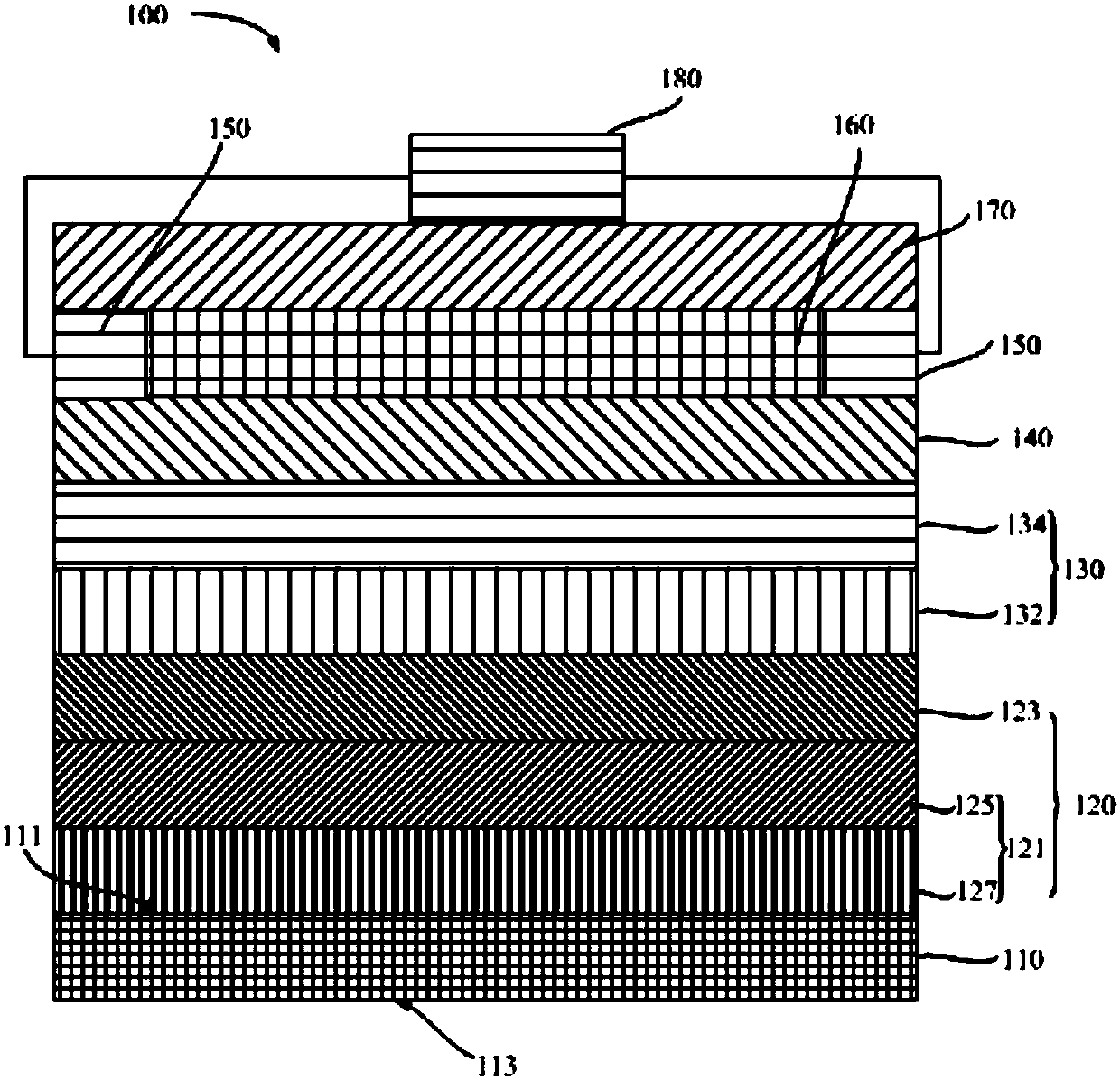
[0061] The method for preparing the above-mentioned colored photovoltaic module 100 includes the following steps:
[0062]S210 , preparing a functional layer 121 on the surface of the transparent substrate 110 .
[0063] The functional layer 121 includes a high refractive index layer 125 and a low refractive index layer 127 .
[0064] In one embodiment, the functional layer 121 is prepared on the substrate by magnetron sputtering. Preferably, the functional layer 121 is prepared by off-line PVD magnetron sputtering.
[0065] Step S220 , preparing a conductive layer 123 on the surface of the functional layer 121 to obtain a colored transparent conductive film 120 laminated on the surface of the transparent substrate 110 .
[0066] In one embodiment, the conductive layer 123 is prepared by magnetron sputtering. The conductive layer 123 is preferably prepared by off-line PVD magnetron sputtering.
[0067] Preferably, the material, manufacturing process and manufacturing param...
Embodiment 1
[0093] 1. On the 3.20mm ultra-clear glass substrate, deposit the high refractive index layer and the low refractive index layer of the functional layer in sequence. Among them, the high refractive index layer is deposited by direct current sputtering of ITO planar target, and the sputtering conditions are: argon 1000 sccm, oxygen 30 sccm, sputtering power 5 kW, target base distance 6.0 cm, substrate temperature 300 °C; low refractive index layer is made of Made of Si rotating target, 40kHz AC power sputtering deposition, the sputtering conditions are: argon 600sccm, oxygen 400sccm, sputtering power 10kW, target base distance 6.0cm. Then, a conductive layer was deposited on the low refractive index layer by direct current sputtering of an ITO planar target to obtain colored TCO glass. 300°C.
[0094] The colored TCO glass of Example 1 is blue-gray, and its structure is ultra-clear glass (3.20mm) / ITO (16.58nm) / SiO 2 (27.72nm) / ITO(150.00nm), wherein, " / " indicates a stacked str...
Embodiment 2
[0100] 1. Deposit the low refractive index layer and the high refractive index layer of the functional layer on the 3.20mm ultra-clear glass substrate. Among them, the low refractive index layer is deposited by sputtering with Si rotating target and 40kHz AC power supply. The sputtering conditions are: argon gas 600sccm, oxygen 400sccm, sputtering power 10kW, target base distance 6.0cm. The high-refractive index layer was deposited on the low-refractive-index layer by direct current sputtering of an ITO planar target. The sputtering conditions were: argon 1000 sccm, oxygen 20 sccm, sputtering power 5 kW, target base distance 6.0 cm, and substrate temperature 400 °C. Then, on the low refractive index layer of the functional layer, use the ITO planar target to deposit the conductive layer by direct current sputtering to obtain colored TCO glass. The sputtering conditions are: argon gas 1000 sccm, oxygen gas 20 sccm, sputtering power 5kW, target base distance 6.0cm , The substrat...
PUM
| Property | Measurement | Unit |
|---|---|---|
| thickness | aaaaa | aaaaa |
| thickness | aaaaa | aaaaa |
| thickness | aaaaa | aaaaa |
Abstract
Description
Claims
Application Information


