Sensor microsystem package method and sensor microsystem

A packaging method and microsystem technology, applied in the direction of microstructure devices, processing microstructure devices, TV system components, etc., can solve the problems of poor versatility, low precision, and large volume of sensor microsystems, and achieve size reduction, High versatility and the effect of improving work performance

Pending Publication Date: 2019-06-28
北京万应科技有限公司
View PDF0 Cites 0 Cited by
  • Summary
  • Abstract
  • Description
  • Claims
  • Application Information

AI Technical Summary

Problems solved by technology

[0009] The purpose of the present invention is to overcome the poor versatility of the sensor microsystem packaging method in the prior art, the large volume of the sensor microsystem, and the shortcomings of low precision, and provide a sensor microsystem packaging method and sensor microsystem

Method used


Image

  • Sensor microsystem package method and sensor microsystem
  • Sensor microsystem package method and sensor microsystem
  • Sensor microsystem package method and sensor microsystem

Examples


Embodiment 1

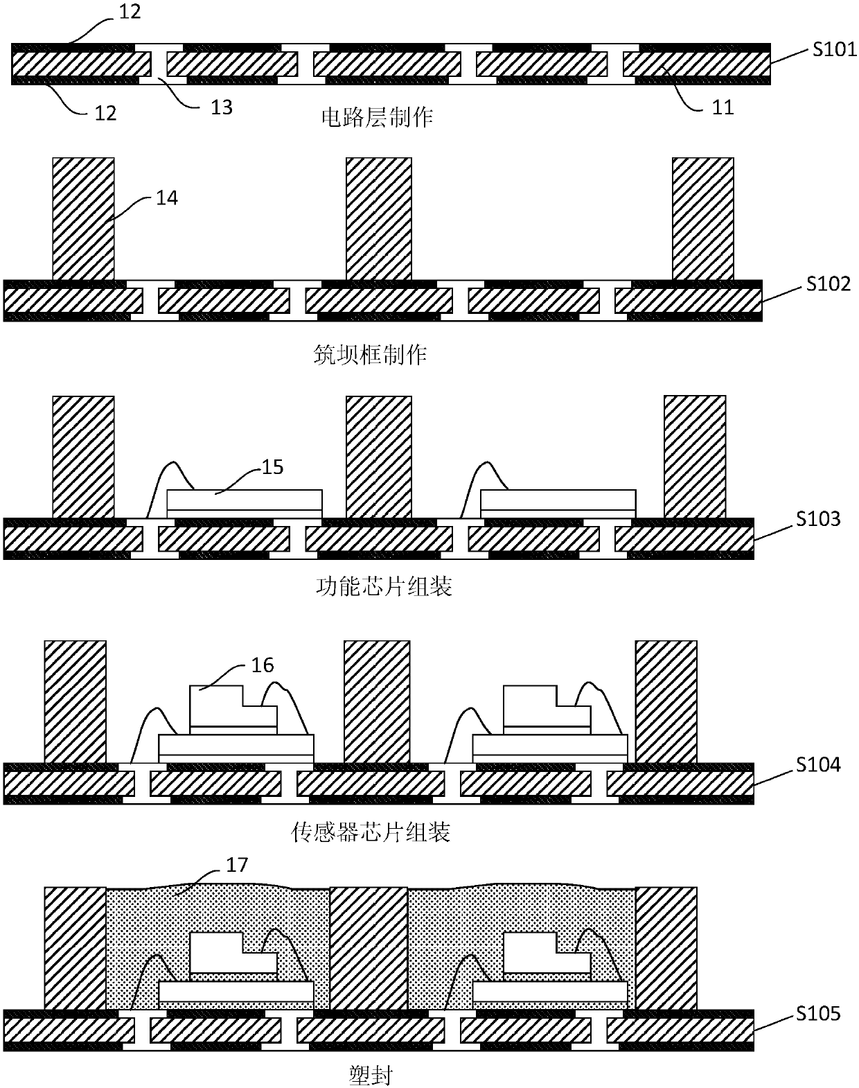
[0039] Such as figure 1 as shown, figure 1 It is a schematic workflow diagram of a sensor microsystem packaging method provided by an embodiment of the present invention, including:

[0040] Step S101: Fabricate a circuit layer 12 covering the substrate 11 on the front and back of the substrate 11, and fabricate a metal through hole 13 that penetrates the substrate 11 and is electrically connected to the circuit layer 12 on the back of the substrate 11;

[0041] Step S102: making a plurality of damming frames 14 for fixing the function chip 15 and the sensor chip 16 on the circuit layer 12 on the front side of the substrate 11;

[0042] Step S103: Between every two damming frames 14, assemble and electrically interconnect the back of the functional chip 15 and the top of the circuit layer 12, the functional chip 15 includes a processor chip or a controller chip;

[0043] Step S104: assembling and interconnecting the back of the sensor chip 16 and the front of the functional ...

Embodiment 2

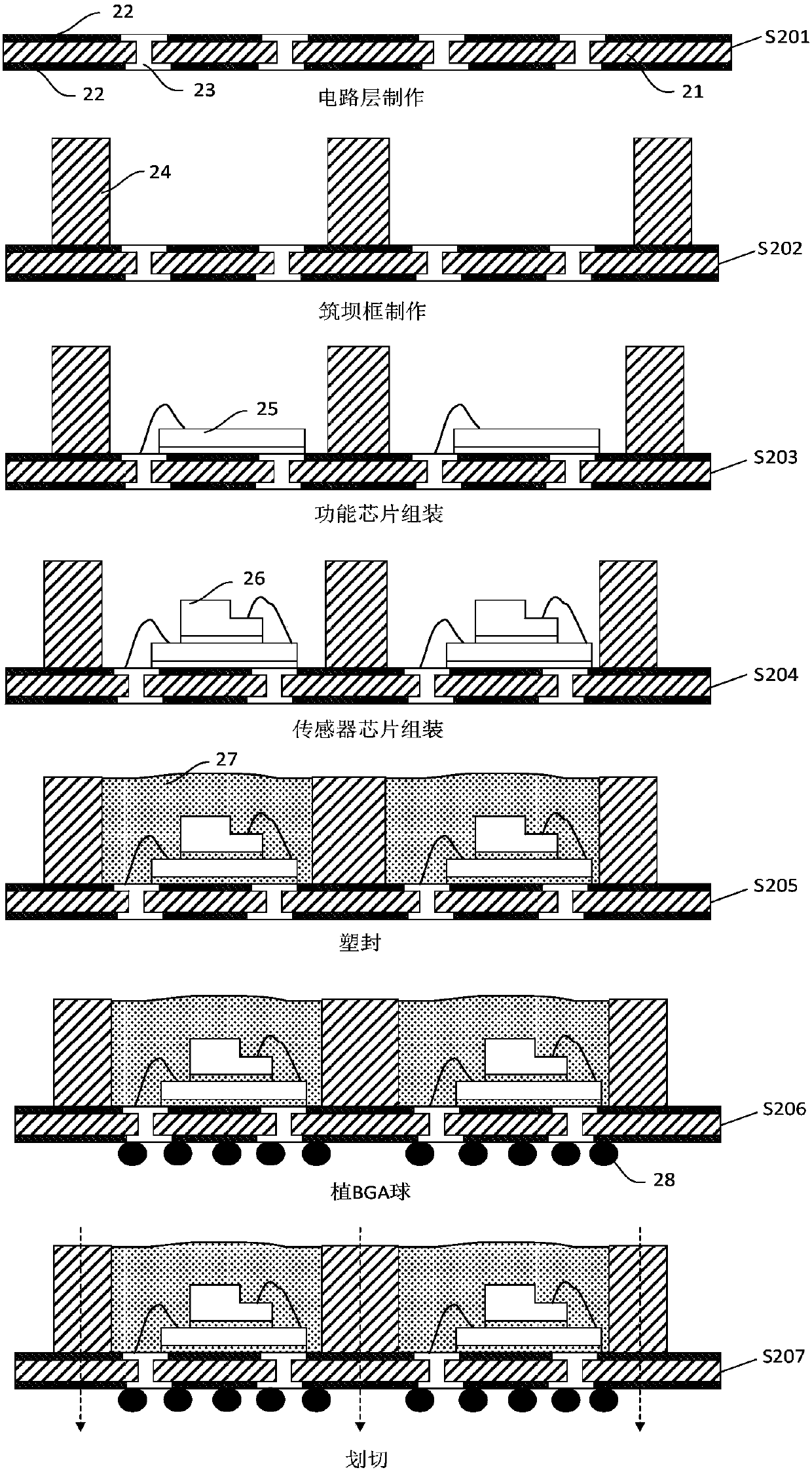
[0058] On the basis of Embodiment 1, Embodiment 2 further adds the fabrication of solder ball array balls, so the same parts as Embodiment 1 will not be repeated. Such as figure 2 as shown, figure 2 It is a schematic workflow diagram of a sensor microsystem packaging method provided by an optional embodiment of the present invention, including:

[0059] Step S201: Fabricate a circuit layer 22 covering the substrate 21 on the front and back of the substrate 21, and fabricate a metal through hole 23 that penetrates the substrate 21 and is electrically connected to the circuit layer 22 on the back of the substrate 21;

[0060] Step S202: making a plurality of damming frames 24 for fixing the function chip 25 and the sensor chip 26 on the circuit layer 22 on the front side of the substrate 21;

[0061] Step S203: Between every two damming frames 24, assemble and electrically interconnect the back of the functional chip 25 and the top of the circuit layer 22, and the functional...

Embodiment 3

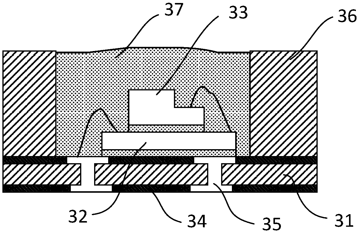
[0071] Embodiment 3 corresponds to Embodiment 1, so the same parts as Embodiment 1 will not be repeated. Such as image 3 as shown, image 3 It is a structural schematic diagram of a sensor microsystem provided by an embodiment of the present invention, including: a substrate 31, a functional chip 32 and a sensor chip 33, the functional chip 32 includes a processor chip or a controller chip, and the front and back of the substrate 31 are respectively set There is a circuit layer 34 covering the substrate 31. The back side of the substrate 31 is provided with a metal through hole 35 that penetrates the substrate 31 and is electrically connected to the circuit layer 34. The circuit layer 34 on the front side of the substrate 31 is provided with a plurality of chips 32 for fixing functions. and the damming frame 36 of the sensor chip 33, the back side of the functional chip 32 is electrically connected to the top of the circuit layer 34, the back side of the sensor chip 33 is el...


PUM


Abstract

The present invention discloses a sensor microsystem and a package method thereof. The method comprises the steps of: respectively manufacturing circuit layers covering a substrate at the front surface and the back surface of the substrate, and manufacturing metal through holes penetrating the substrate and electrically connected with the circuit layers at the back surface of the substrate; manufacturing a plurality of damming frames configured to fix a functional chip and a sensor chip on the circuit layer at the front surface of the substrate; assembling and electrically and mutually connecting the back surface of the functional chip and the top portions of the circuit layers between every two damming frames, wherein the functional chip comprises a processor chip or a controller chip; assembling and mutually connecting the back surface of the sensor chip and the front surface of the functional chip; filling the position between every two damming frames with flexible glue or silica gel covering the functional chip and the sensor chip to obtain a sensor microsystem wafer comprising the functional chip and the sensor chip. According to the invention, the sensor microsystem-level package is achieved, the working performance is high, the stress is low, and the universality is high.

Description

technical field [0001] The invention relates to the technical field of microelectronic packaging, in particular to a sensor microsystem packaging method and a sensor microsystem. Background technique [0002] A sensor is a detection device that can sense the measured information and convert the sensed information into electrical signals or other required forms of information output according to certain rules to meet the requirements of information transmission, processing, storage, and display. , recording and control requirements. In modern industrial production, especially in the automated production process, various sensors are used to monitor and control various parameters in the production process, so that the equipment can work in a normal or optimal state, and the product can achieve the best quality. [0003] With the continuous development of various electronic products in the direction of high integration, high performance, light weight and miniaturization, sensor...

Claims


Application Information

Patent Timeline
Patent Type & Authority Applications(China)
IPC IPC(8): H01L25/18H01L23/535B81B7/02B81C3/00
Inventor 黄玲玲
Owner 北京万应科技有限公司
Why Eureka
Try Eureka