Electrostatic transfer head and manufacturing method thereof

A technology of electrostatic transfer and manufacturing method, which is applied in the manufacture of circuits, electrical components, semiconductors/solid-state devices, etc., and can solve problems such as low process yield, insufficient suction, and poor uniformity of glue

Active Publication Date: 2019-07-09
NANJING CEC PANDA LCD TECH
View PDF5 Cites 6 Cited by
  • Summary
  • Abstract
  • Description
  • Claims
  • Application Information

AI Technical Summary

Problems solved by technology

[0010] In order to solve the problems of the existing transfer head with raised edges, poor glue uniformity, insufficient suction and low process yield due to edge leakage, the present invention provides the following technical solutions:

Method used


Image

  • Electrostatic transfer head and manufacturing method thereof
  • Electrostatic transfer head and manufacturing method thereof
  • Electrostatic transfer head and manufacturing method thereof

Examples


Embodiment 1

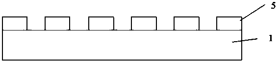
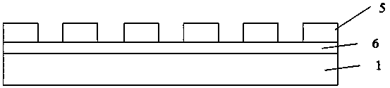
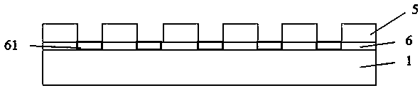
[0045] Such as Figure 8 As shown, Embodiment 1 of the present invention provides an electrostatic transfer head, including a substrate 1 , a patterned first metal layer 21 on the substrate 1 , and a dielectric layer 3 on the first metal layer 21 . Wherein the substrate 1 has a plurality of recesses 11 and a plurality of protrusions 12 arranged alternately, the dielectric layer 3 includes a first cavity 33 corresponding to the recesses 11, the first metal layer 21 is embedded in the protrusions 12 of the substrate 1, the second The upper surface of a metal layer 21 is flush with the upper surface of the substrate 1 .

[0046] Further, the dielectric layer 3 may be a one-layer or multi-layer structure, preferably, the dielectric layer 3 is a two-layer structure, the dielectric layer 3 includes a first dielectric layer 31 and a second dielectric layer 32, the first dielectric layer The electrical layer 31 is located on the second dielectric layer 32, the second dielectric layer...


PUM


Abstract

The invention provides an electrostatic transfer head and a manufacturing method thereof and belongs to the technical field of Micro LED massive transfer. The transfer head includes a substrate, a first patterned metal layer and a dielectric layer, wherein the substrate includes a concave portion and a convex portion, the dielectric layer includes a first concave hole corresponding to the concaveportion, and the first metal layer is embedded in the substrate. The transfer head is advantaged in that the metal is embedded in the substrate or a flat layer, problems of rim projection, poor glue distribution uniformity, insufficient absorption due to edge leakage and low process yield rate of a transfer head in the prior art are solved, and different micro elements can be transferred without obstruction while massive transfer is better completed.

Description

technical field [0001] The invention belongs to the technical field of Micro LED mass transfer, and in particular relates to an electrostatic transfer head and a manufacturing method thereof. Background technique [0002] Micro LED Display has the advantages of high efficiency, high brightness, high reliability, energy saving, small size, and small thickness. It is a new generation of display technology. In the Micro LED manufacturing process, epitaxial wafers need to be fabricated into LEDs one by one through a series of processes, and then transferred to the TFT backplane. Because the size of the LED is extremely small, the number of LEDs that need to be transferred to the TFT backplane to form a Micro LED Display is extremely large. This technology of transferring a particularly large number of micro components from one substrate to another is called giant. volume transfer. [0003] Mass transfer is currently the main bottleneck of Micro LED production. How to solve th...

Claims


Application Information

Patent Timeline
Patent Type & Authority Applications(China)
IPC IPC(8): H01L21/683H01L33/00
CPCH01L21/6833H01L33/0095
Inventor 安金鑫朱充沛张惟诚王俊星张良玉高威
Owner NANJING CEC PANDA LCD TECH
Why Eureka
Try Eureka