Eureka AIR delivers breakthrough ideas for toughest innovation challenges, trusted by R&D personnel around the world.

Signal terminal embedded power semiconductor module and packaging processing thereof

A technology of power semiconductors and signal terminals, which is applied in the direction of semiconductor devices, semiconductor/solid-state device manufacturing, semiconductor/solid-state device components, etc., can solve the problems of terminal load-carrying capacity to be improved, achieve simplified structure and manufacturing process, and improve practicability Effect

Pending Publication Date: 2019-07-12
合肥中恒微半导体有限公司
View PDF0 Cites 3 Cited by
  • Summary
  • Abstract
  • Description
  • Claims
  • Application Information

AI Technical Summary

Problems solved by technology

For existing high-power semiconductor devices, the terminal carrying capacity needs to be improved

Method used


Image

  • Signal terminal embedded power semiconductor module and packaging processing thereof
  • Signal terminal embedded power semiconductor module and packaging processing thereof
  • Signal terminal embedded power semiconductor module and packaging processing thereof

Examples


Embodiment 1

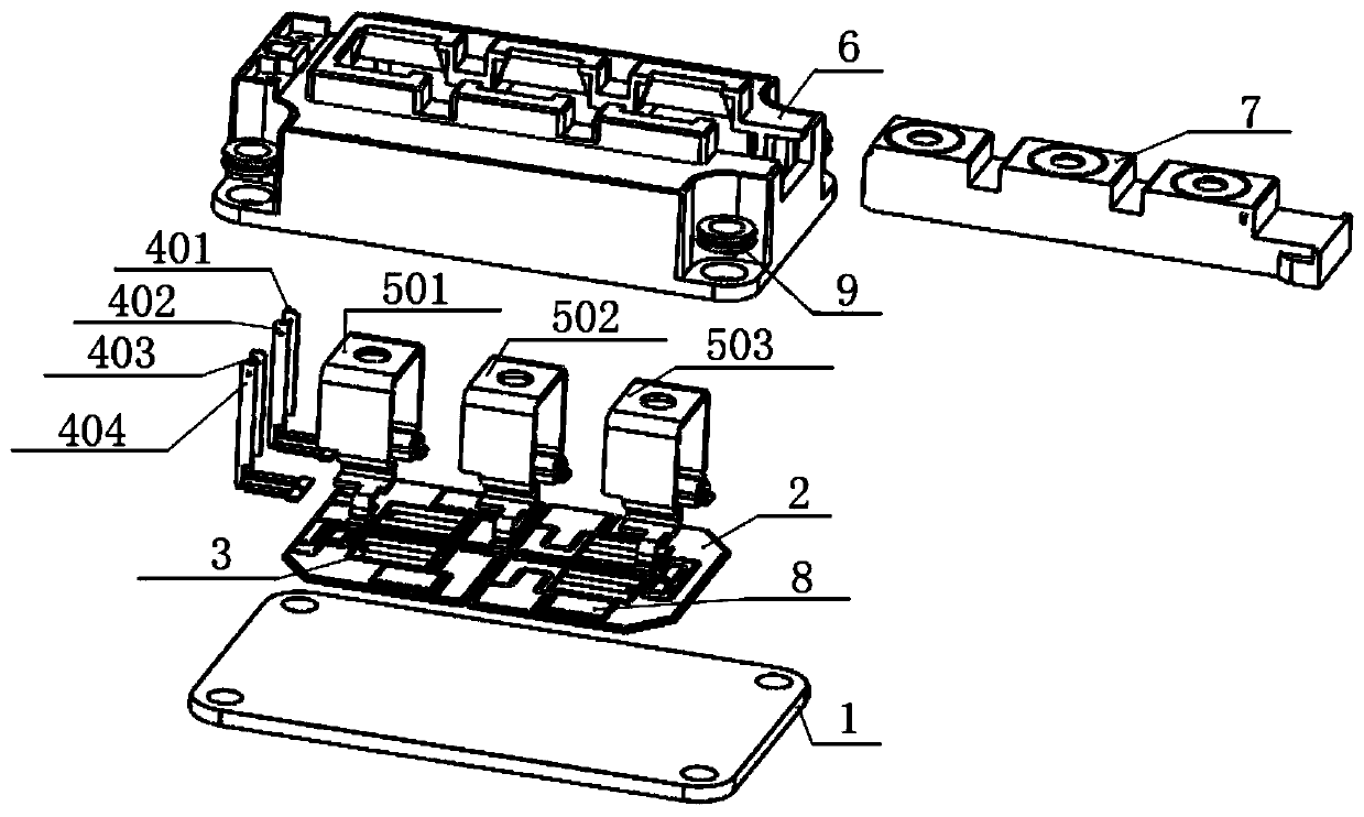
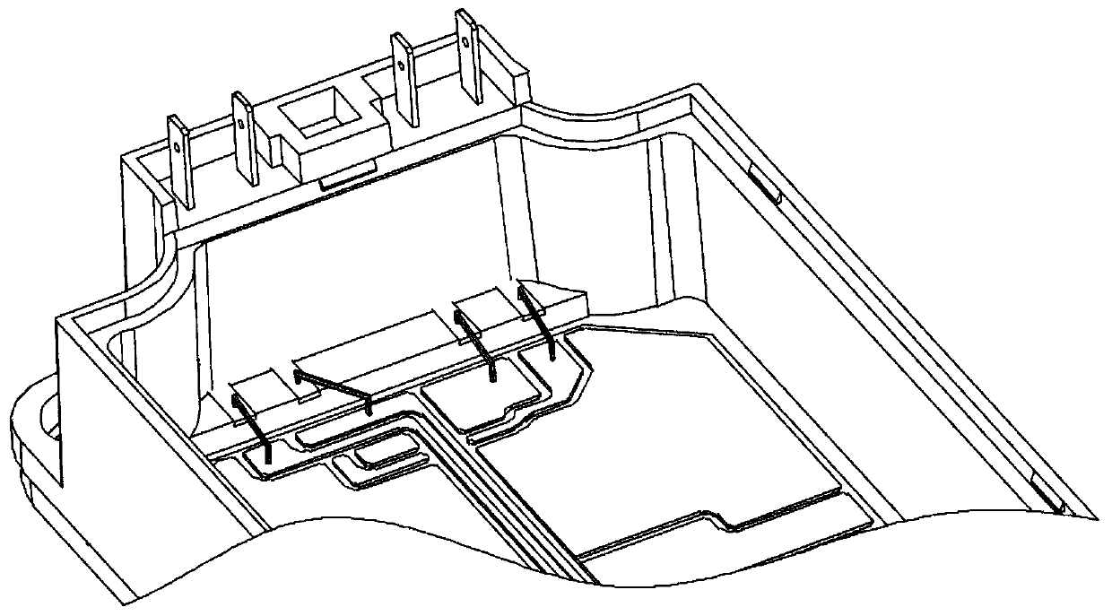
[0018] A signal terminal embedded power semiconductor module, taking the IGBT module as an example, such as figure 1 , figure 2 As shown, it includes a heat dissipation copper plate 1, a ceramic copper clad plate 2 arranged on the heat dissipation copper plate, a power semiconductor chip 3 mounted on the ceramic copper clad plate, and four signal terminals 401- 404 and three power terminals 501-503, and a housing; the housing includes an outer shell 6 and a plug 7, and the plug 7 is inserted into the gap between the two legs of the power terminal; the ceramic copper clad plate Other electronic components, such as diodes 8 , are also welded on it; The signal terminal and the power terminal are made of copper, and the surface is plated with aluminum, silver or nickel. The design of the plug makes it possible to complete the packaging by pushing and pulling, which is more convenient to operate and easy to disassemble and maintain.

[0019] The signal terminals are injection-m...

Embodiment 2

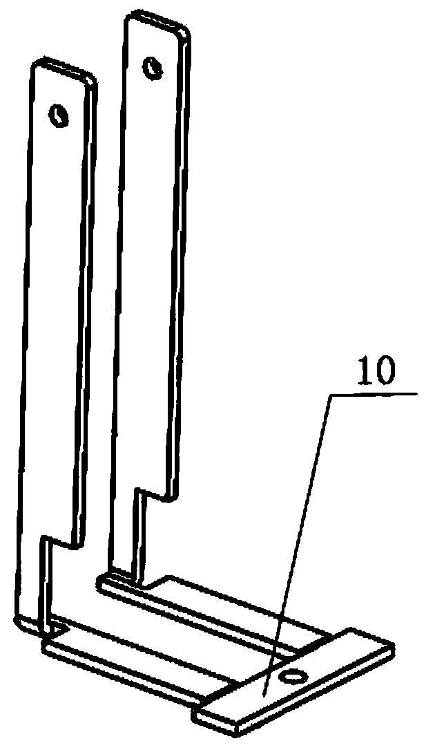
[0025] A packaging process for a signal terminal embedded power semiconductor module, in which two adjacent signal terminals are connected through a connecting bridge, and then integrated with the housing through an injection molding process; after the injection molding process is completed, the connection bridge broken;

[0026] Specifically include the following steps:

[0027] S1: The signal terminal with the connecting bridge is injection molded into one body with the housing;

[0028] S2: Solder the power semiconductor chips and power terminals on the ceramic copper clad board;

[0029] S3: Solder the ceramic copper clad laminate to the heat dissipation copper plate;

[0030] S4: Break off the connection bridge at the bottom of the signal terminal that is integrally molded with the housing, and weld it to the ceramic copper clad board through a bonding process, and adjust the positional relationship between the housing, the heat dissipation copper plate and the power te...


PUM


Abstract

The invention discloses a signal terminal embedded power semiconductor module, comprising a heat dissipating copper board, a ceramic copper-clad board disposed on the heat dissipating copper board, apower semiconductor chip mounted on the ceramic copper-clad board, signal terminals and power terminals which are connected to the ceramic copper-clad board, and a casing, wherein every two adjacent signal terminals are injection-molded in parallel, and are integrally formed with the casing by an injection molding process; the lower end of each signal terminal is connected to the ceramic copper-clad board by a bonding process; the upper end of each ceramic copper-clad board is connected to an external electrical system; the power terminals use a symmetrical branch structure, and the two pins are recessed inward to form a certain arc; the signal terminals and the power terminals are formed by a punching and bending mechanical process. The practicability of the signal terminals of the powersemiconductor module is improved, the soldering efficiency of the power terminals and the signal terminals are improved, and the structure and the manufacturing process are simplifed.

Description

technical field [0001] The invention relates to the technical field of power semiconductor devices, in particular to a signal terminal embedded power semiconductor module and a packaging process thereof. Background technique [0002] At present, power modules are widely used in power electronic circuits, and are usually packaged in semiconductors. Power semiconductor packaging technology includes material selection, structural design, process design, packaging technology and other issues. Many power chips are packaged into modules in a more beautiful and well-proportioned layout through calibration and calculation. The packaging process needs to consider the current balance of the device, the heat dissipation of the chip and the simplification of the process steps. For existing high-power semiconductor devices, the carrying capacity of terminals needs to be improved. Contents of the invention [0003] In view of the above problems, the present invention provides a signal...

Claims


Application Information

Patent Timeline
Patent Type & Authority Applications(China)
IPC IPC(8): H01L23/492H01L21/56H01L21/48
CPCH01L23/4926H01L21/56H01L21/4882H01L2924/19107
Inventor 袁磊
Owner 合肥中恒微半导体有限公司
Why Eureka
Eureka Blog
Learn More