Method for processing laminated chip type electronic component

A technology of electronic components and processing methods, which is applied in the direction of electrical components, multi-layer circuit manufacturing, printed circuits, etc., can solve the problems that affect the appearance reliability of processed and formed devices, the surface defect of the substrate, and the lack of material strength, etc., to achieve low cost, Prevents cutting damage and protects the substrate surface

Active Publication Date: 2019-07-12
东莞顺络钽电容电子有限公司
View PDF10 Cites 3 Cited by
  • Summary
  • Abstract
  • Description
  • Claims
  • Application Information

AI Technical Summary

Problems solved by technology

However, the laminated substrate in the prior art is prone to defects near the surface of the substrate in the subsequent cutting process due to insu

Method used


Image

  • Method for processing laminated chip type electronic component
  • Method for processing laminated chip type electronic component

Examples


Embodiment Construction

[0023] The principles and features of the present invention will be described below in conjunction with the accompanying drawings, and the examples given are only used to explain the present invention, and are not used to limit the scope of the present invention.

[0024] It should be noted that the orientation terms such as left, right, up, down, top, and bottom in this embodiment are only relative concepts, or refer to the normal use status of the product, and should not be regarded as having restrictive.

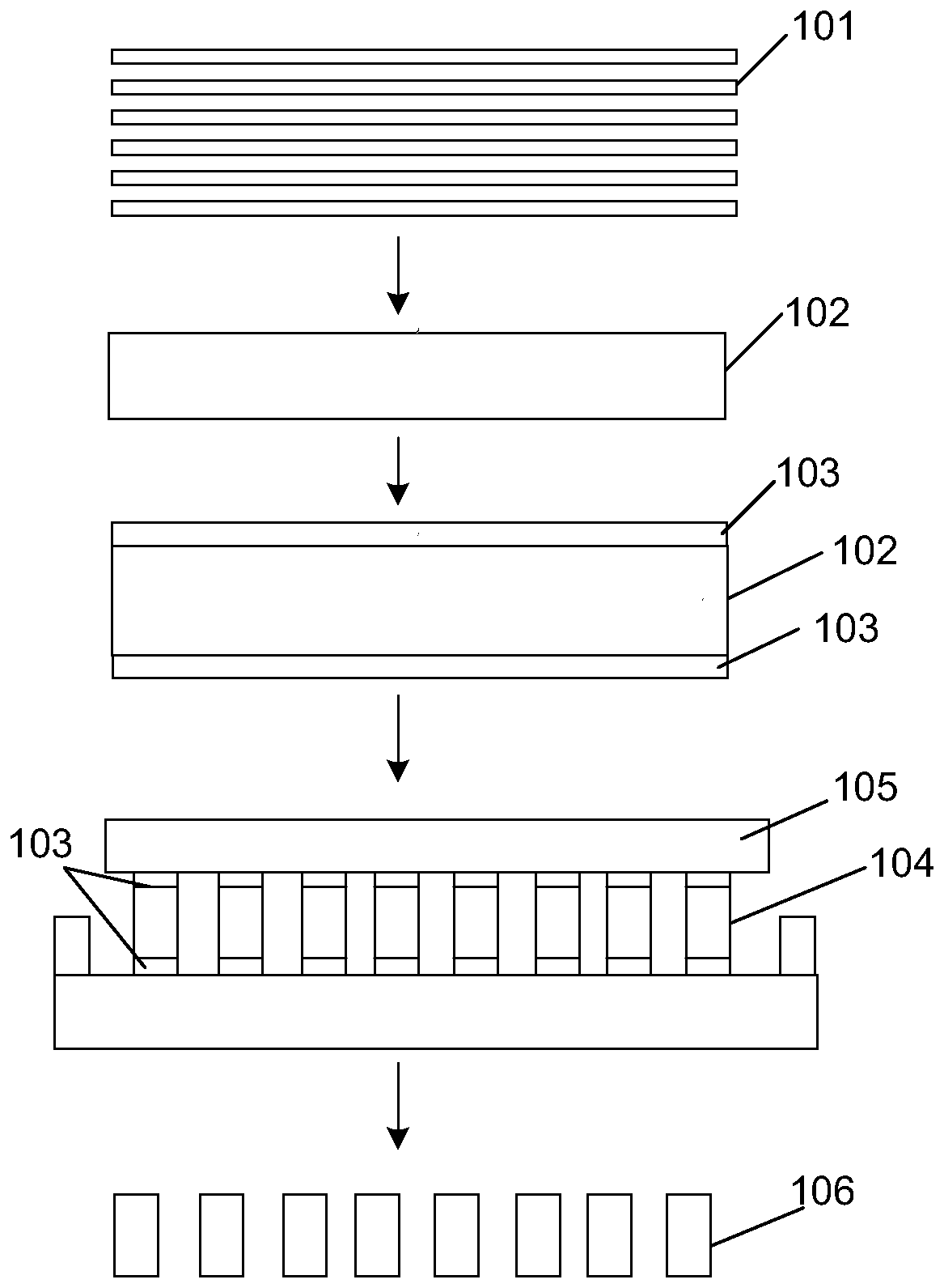
[0025] Such as figure 1 As shown, a processing method of laminated chip electronic components (hereinafter referred to as "components"), in a specific embodiment, the processing method includes the following steps:

[0026] S1. Laminate at least one layer of carbon-based sacrificial sheets on the upper and lower surfaces of the multilayer substrate. The multilayer substrate is processed by a plurality of single-layer green ceramic sheets with circuits printed on the surf...


PUM

PropertyMeasurementUnit
Thicknessaaaaaaaaaa

Abstract

The invention discloses a method for processing a laminated chip type electronic component. The method comprises the steps of (S1) separately stacking at least one layer of carbon-based sacrificial sheet on upper and lower surfaces of a multi-layer substrate, wherein the multi-layer substrate is formed by processing multiple single-layer raw porcelain pieces, and circuits are printed on the surfaces of the single-layer raw porcelain pieces, (S2) performing isostatic pressing on a product formed in step (S1), (S3) cutting the product which is subjected to isostatic pressing in step (S2) into asingle component, and (S4) sintering a product cut in step (S3) to obtain the laminated chip type electronic component after the carbon-based sacrificial sheets are completely decomposed and disappearduring the sintering process. According to the method, the cutting damage can be prevented, the adding of new equipment in a production line is not needed, and the method has the advantages of low cost and high efficiency and is suitable for the mass processing of existing laminated chip type electronic components.

Description

technical field [0001] The invention relates to the processing of electronic components, in particular to a processing method of laminated electronic components. Background technique [0002] Low Temperature Co-fired Ceramic (LTCC) technology is an eye-catching integrated component technology developed in recent years. It has become the mainstream technology of passive integration and has the advantages of good consistency and high precision. In the LTCC production process, lamination is an important step in realizing the formation of a single-layer raw ceramic printed circuit to a multi-layer circuit body, and it is also an important process that affects the surface morphology. However, the laminated substrates in the prior art are prone to defects near the surface of the substrate in the subsequent cutting process due to insufficient material strength or the influence of the lamination process, which affects the appearance and reliability of processed and formed devices. ...

Claims


Application Information

Patent Timeline
IPC IPC(8): H05K3/46H05K3/22
CPCH05K3/22H05K3/4611
Inventor 苏柯铭李志龙李威
Owner 东莞顺络钽电容电子有限公司
Why Eureka
Try Eureka