Chemical mechanical planarization device and wafer transmission method

A chemical-mechanical and flattening technology, applied in metal processing equipment, grinding/polishing equipment, surface polishing machine tools, etc., can solve the problems of complex structure of transmission mechanism and low efficiency of wafer transmission, so as to improve transmission efficiency and efficiency The effect of increasing and reducing the probability of damage

Pending Publication Date: 2019-07-19
HANGZHOU ZHONGGUI ELECTRONICS TECH CO LTD
View PDF2 Cites 19 Cited by
  • Summary
  • Abstract
  • Description
  • Claims
  • Application Information

AI Technical Summary

Problems solved by technology

[0009] One of the objectives of the present invention is to propose a new type of chemical mechanical planarization equipment with a polishing unit array layout for the problems of low wafer transmission efficiency and complex structure of the transmission mechanism in the existing chemical mechanical planarization equipment, and based on the array layout A wafer transfer module is proposed, which is arranged above the polishing unit array, so that the wafer transfer unit of the wafer transfer module can pass through the polishing unit at any time without being disturbed

Method used


Image

  • Chemical mechanical planarization device and wafer transmission method
  • Chemical mechanical planarization device and wafer transmission method
  • Chemical mechanical planarization device and wafer transmission method

Examples


Embodiment Construction

[0054] The present invention will be further described below through specific embodiments in conjunction with the accompanying drawings. These embodiments are only used to illustrate the present invention, and are not intended to limit the protection scope of the present invention.

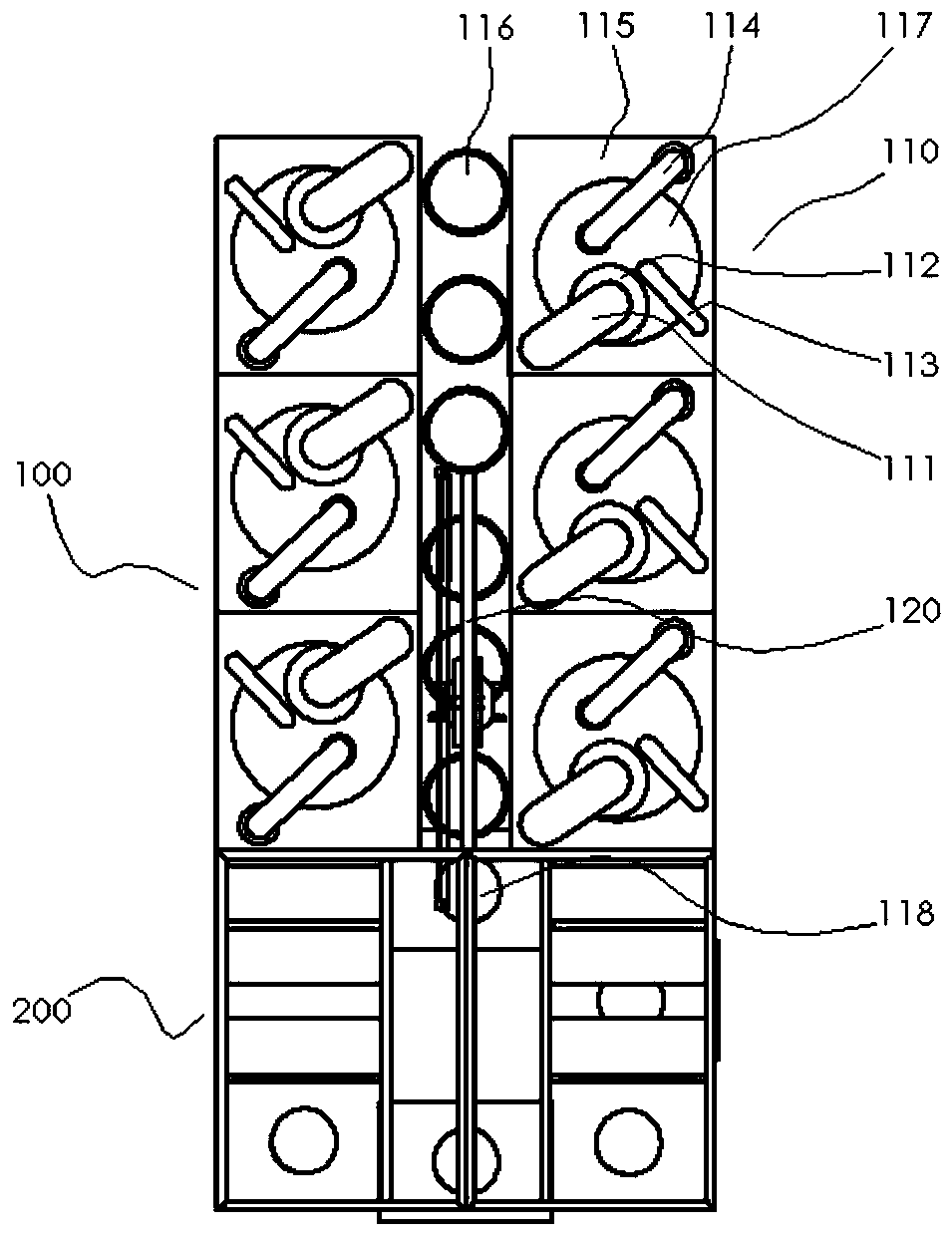
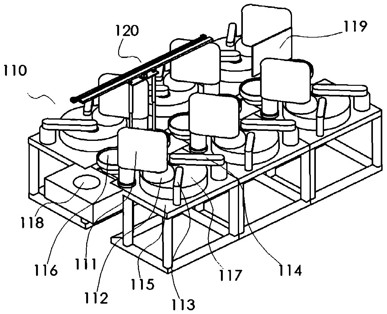
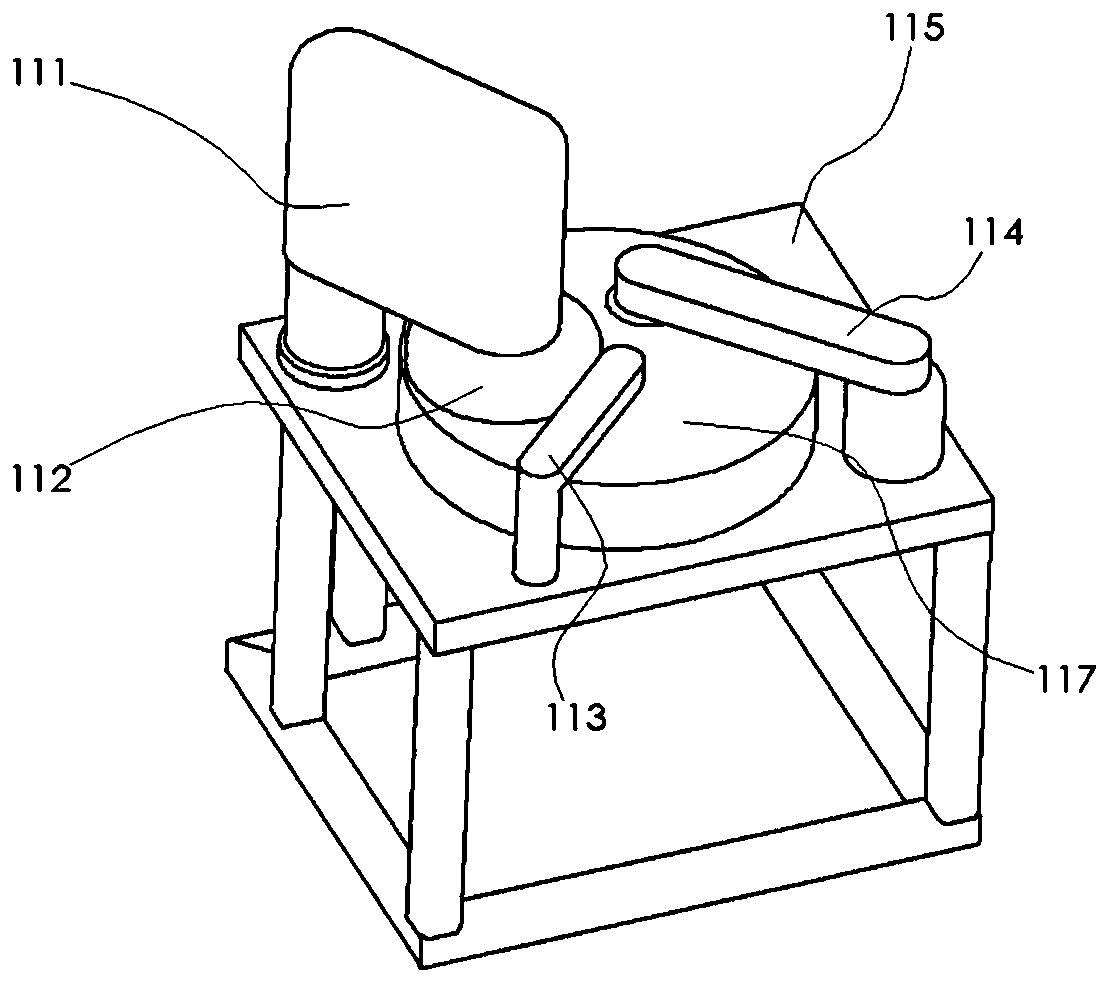
[0055] The chemical mechanical planarization device according to the present invention includes a polishing module composed of a plurality of polishing units and a plurality of cleaning modules. Each polishing unit includes a workbench, a polishing disc, a polishing head, a polishing arm, a dresser, a polishing liquid arm, and the like. Multiple polishing loading tables are arranged on one side of the multiple polishing units. The polishing disk, polishing head, polishing arm, dresser, and polishing liquid arm are arranged on the workbench according to the processing position. The polishing arm can carry the polishing head to move between the polishing disc and the polishing loading table. The t...


PUM


Abstract

The invention discloses a chemical mechanical planarization device and a wafer transmission device and method. The wafer transmission device comprises at least one wafer polishing transmission mechanical arm, the wafer polishing transmission mechanical arm comprises a horizontal transmission mechanism, a vertical transmission mechanism and a wafer grabbing device, a polishing transfer table, a cleaning transfer table and a polishing loading table are arranged in the movable range, in the horizontal straight line moving direction, of the wafer grabbing device, according to the wafer transmission device, the wafer can be directly transmitted among the polishing transfer table, the polishing loading table and the cleaning transfer table, due to the fact that transfer is not needed, the wafertransfer frequency is reduced, the wafer transmission time is shortened, the transmission efficiency is improved, and the probability of damage generated by wafer transmission is reduced. Due to layout of the chemical mechanical planarization device, the transmission stroke is reduced, and machining efficiency of the chemical mechanical planarization device is obviously improved on year-on-year basis.

Description

technical field [0001] The invention relates to the technical field of semiconductor equipment, in particular to chemical mechanical planarization equipment, wafer transmission equipment and a wafer transmission method. Background technique [0002] With the rapid development of the semiconductor industry, the feature size of integrated circuits tends to be miniaturized, so the high planarization of the semiconductor thin film surface has an important impact on the high performance, low cost and high yield of the device. [0003] Chemical mechanical polishing (Chemical Mechanical Planarization, CMP) technology is a combination of chemical action and mechanical action. Its working principle is that first, the surface material of the workpiece reacts chemically with the oxidant and catalyst in the polishing liquid to form a soft layer that is relatively easy to remove, and then removes the soft layer under the mechanical action of the abrasive and the polishing pad in the poli...

Claims


Application Information

Patent Timeline
Patent Type & Authority Applications(China)
IPC IPC(8): B24B29/02B24B41/00B24B41/06
CPCB24B29/02B24B41/005B24B41/06
Inventor 李苍顾静然朱铭
Owner HANGZHOU ZHONGGUI ELECTRONICS TECH CO LTD
Why Eureka
Try Eureka