Array substrate repairing method, array substrate, display panel and display device

An array substrate and repair method technology, applied in nonlinear optics, instruments, optics, etc., can solve the problem that the gate line cannot control the signal input and output of the pixel unit, the data line and the drain of the switching diode are short-circuited, and the control process of the pixel unit fails. and other problems to achieve the effect of maintaining normal display function, preventing control failure, and reducing the incidence of poor wiring.

Active Publication Date: 2019-07-19
CHENGDU ZHONGDIAN PANDA DISPLAY TECH CO LTD
View PDF5 Cites 4 Cited by
  • Summary
  • Abstract
  • Description
  • Claims
  • Application Information

AI Technical Summary

Problems solved by technology

[0004] However, in the above-mentioned repair process, the trace of the repair line will be in contact with the drain, so that the data line and the drain of the switching diode are short-circuited, which directly causes the gate line to be unable to control the signal input and output of the pixel unit, and the pixel unit control process fail
And in the pixel dark point operation process, in order to ensure the normal pixel dark point, will use image 3 The cutting process shown cuts off the part of the drain that is in contact with the repair line. However, this cannot avoid the short connection between the drain and the common line, which will cause poor connection of the dark point operation and affect the display effect of the pixel unit.

Method used


Image

  • Array substrate repairing method, array substrate, display panel and display device
  • Array substrate repairing method, array substrate, display panel and display device
  • Array substrate repairing method, array substrate, display panel and display device

Examples


Embodiment 1

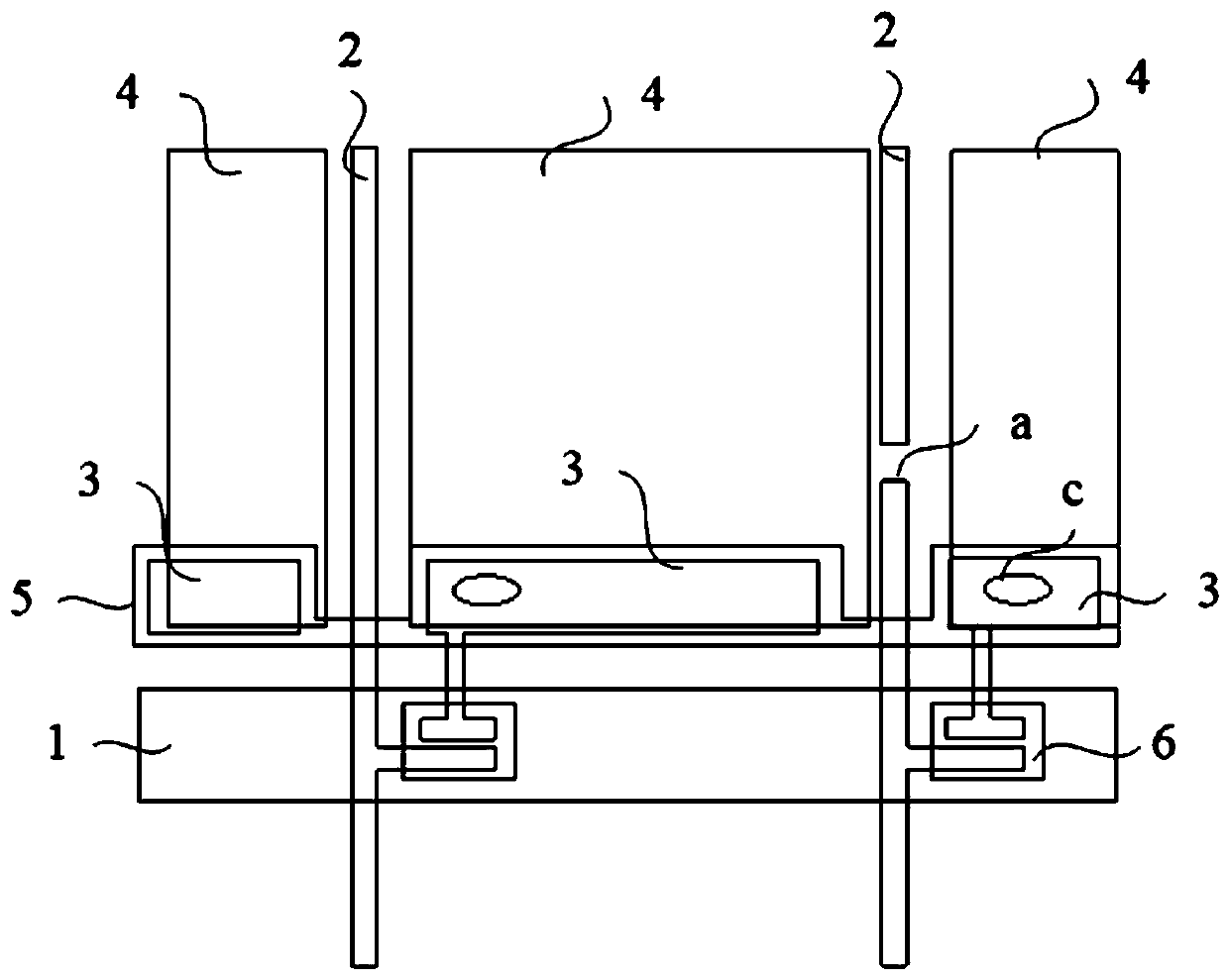
[0067] figure 1 It is a schematic structural diagram of an array substrate with data lines in a fracture area in the prior art. figure 2 It is a schematic structural diagram of an array substrate provided with repair lines in the prior art. image 3 It is a structural schematic diagram of the array substrate after repairing and cutting processes in the prior art. Figure 4 is an equivalent circuit diagram of an array substrate in the prior art. Figure 5 It is an equivalent circuit diagram of an array substrate provided with repair lines in the prior art. Image 6 It is an equivalent circuit diagram of an array substrate operated by a dark spot in the prior art.

[0068] refer to Figure 1 to Figure 6 As shown, in the current array substrate, the data line 2 and the gate line 1 are alternately arranged on the base substrate. Due to the overlapping area of ​​the data line 2 and the gate line 1, the data line 2 is generally stacked on the gate line 1. Therefore, the "climb...

Embodiment 2

[0086] Figure 9 It is a schematic flowchart of the method for repairing an array substrate provided in Embodiment 2 of the present invention. refer to Figure 9 As shown, on the basis of the first embodiment above, the second embodiment of the present invention provides a method for repairing an array substrate, including:

[0087] S1: Determine the break area of ​​the data line.

[0088] It should be noted that due to the overlapping area of ​​the data line and the gate line, the data line is generally stacked above the gate line, so the "climbing" area of ​​the data line is easy to be placed on the substrate due to its low flatness. Breakage occurs during the heat treatment or etching process, affecting normal signal transmission in the data line, so the overlapping area between the data line and the gate line can be used as the fracture area of ​​the data line.

[0089] S2: A repair line is provided on the data line with a fractured area, and two ends of the repaired li...

Embodiment 3

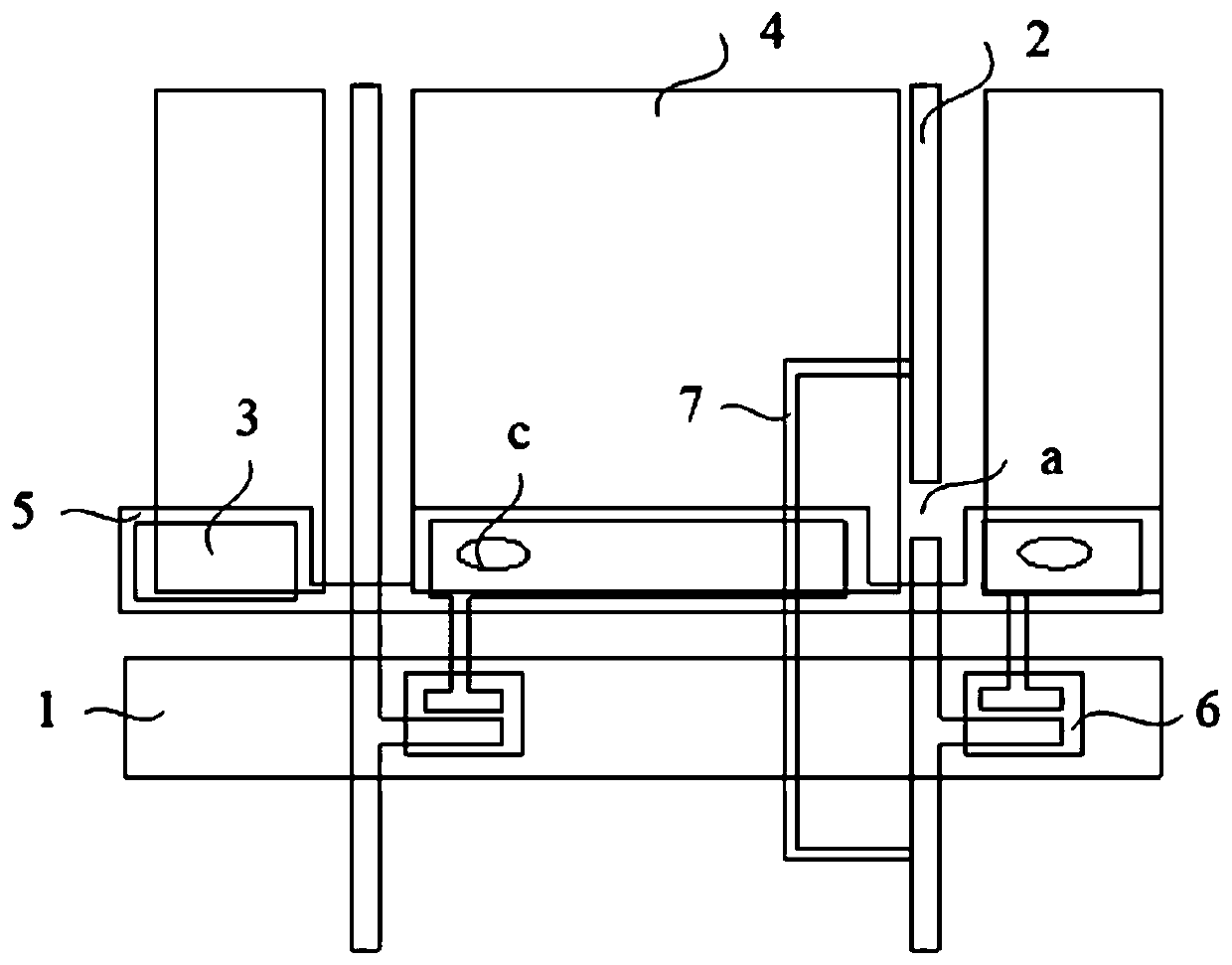
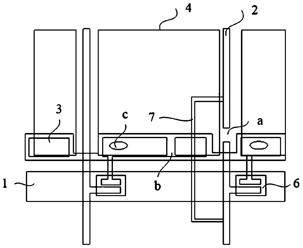
[0098] Figure 10 A schematic structural diagram of an array substrate provided with repair lines provided in Embodiment 3 of the present invention. Figure 11 It is a schematic structural diagram of the array substrate after the dicing process provided by Embodiment 3 of the present invention. Figure 12 An equivalent circuit diagram of the array substrate provided by Embodiment 3 of the present invention. Figure 13 An equivalent circuit diagram of an array substrate provided with repair lines provided in Embodiment 3 of the present invention.

[0099] refer to Figure 10 to Figure 13 , and in combination with Example 1 Figure 7 and Figure 8 As shown, Embodiment 3 of the present invention provides a repaired array substrate, specifically:

[0100] The repaired array substrate is repaired by the above-mentioned repairing method, which specifically includes: a base substrate, on which storage capacitors 80, switching diodes 60, and criss-cross gate lines 10 and data lin...


PUM


Abstract

The invention provides an array substrate repairing method, an array substrate, a display panel and a display device. The array substrate comprises an underlayer substrate, a storage capacitor, switching diodes, grid lines and data lines, and multiple pixel areas are defined by the grid lines and the data lines; capacitance plates are arranged between the common line of the storage capacitor and apixel electrode in each pixel area; the capacitance plates comprise a first capacitance plate and at least one second capacitance plate, the first capacitance plate and the second capacitance plate are separately arranged, the first capacitance plate is close to the switching diode corresponding to the pixel area, and the first capacitance plate is electrically connected with the drain of the switching diode and meanwhile electrically connected with the pixel electrode; and the second capacitance plate is electrically connected with the pixel electrode. According to the method provided by theinvention, the broken area of the data line on the array substrate can be effectively repaired, the normal display function of the pixel unit can be ensured, meanwhile the dark spot operation of thepixel unit is not affected, and the display effects of the display panel and the display device are ensured.

Description

technical field [0001] The present invention relates to the field of display technology, in particular to a method for repairing an array substrate, an array substrate, a display panel and a display device. Background technique [0002] Thin Film Transistor Liquid Crystal Display (TFT-LCD) has the advantages of low power consumption, small size and low radiation. It places liquid crystal between two conductive materials and uses the thin film transistor layer to control the two The electric field between the electrodes is driven to cause the electric field effect of twisting the liquid crystal molecules to control the projection or shading of the light source, so as to achieve the purpose of displaying images. [0003] In the TFT-LCD substrate preparation process, there is an overlapping area between the data line and the gate line, and the data line will produce a "climbing" area in the overlapping area, resulting in poor surface flatness of the data line, and when the subs...

Claims


Application Information

Patent Timeline
Patent Type & Authority Applications(China)
IPC IPC(8): G02F1/1362
CPCG02F1/136213G02F1/136227G02F1/136259G02F1/136286
Inventor 高鹏辛亚男李向峰曾柯雒斌
Owner CHENGDU ZHONGDIAN PANDA DISPLAY TECH CO LTD
Why Eureka
Try Eureka