Programming test device for programmable chip

A test device and chip technology, applied in software testing/debugging, error detection/correction, instruments, etc., can solve problems such as high complexity, low efficiency, and impact on chip life, so as to reduce erroneous operations, improve programming efficiency, and protect The effect of perfect mechanism

Pending Publication Date: 2019-07-19
QI AUTOMOTIVE CO LTD
View PDF0 Cites 1 Cited by
  • Summary
  • Abstract
  • Description
  • Claims
  • Application Information

AI Technical Summary

Problems solved by technology

[0003] The program programmer method needs to use a separate programmer. When the source program needs to be modified, the single-chip microcomputer chip needs to be pulled out from the target board, and then the updated target code is re-solidified into the single-chip microcomputer chip. In this process, It is often necessary to repeatedly plug and unplug the chip, which is troublesome to operate, which affects the life of the chip, and the program writer is generally expensive and the production cost is high
[0004] The serial port / parallel port SPI simulation programming method generally uses the serial port or parallel port to simulate the SPI timing sequence for chip programming. This technology no longer needs to use a programmer, but the error correction capability is poor. Once an error occurs such as data misalignment or buffer error, the computer needs to be restarted. ;The efficiency is low, the programming speed is only about 1.6kbps, and it takes about 15 seconds to program a 2K program, which seriously affects the progress of batch programming
[0005] The original programming implementation method is to use the upper computer to send out the agreed signal of the chip to make the chip enter the programming state. If there is no agreed signal, the chip enters the normal operation state for testing; in this way, it needs to be restarted when switching between the programming state and the normal operation test state. , and it needs to switch between the two states multiple times in programming, which is low in efficiency and high in complexity

Method used


Image

  • Programming test device for programmable chip
  • Programming test device for programmable chip
  • Programming test device for programmable chip

Examples


Embodiment Construction

[0026] Below, the present invention will be further described in conjunction with the accompanying drawings and specific embodiments, the content of which is sufficient to enable any person skilled in the art to understand the technical content of the present invention and implement it accordingly, and according to the claims, description and accompanying drawings disclosed in the present invention , those skilled in the art can easily understand the related objects and advantages of the present invention.

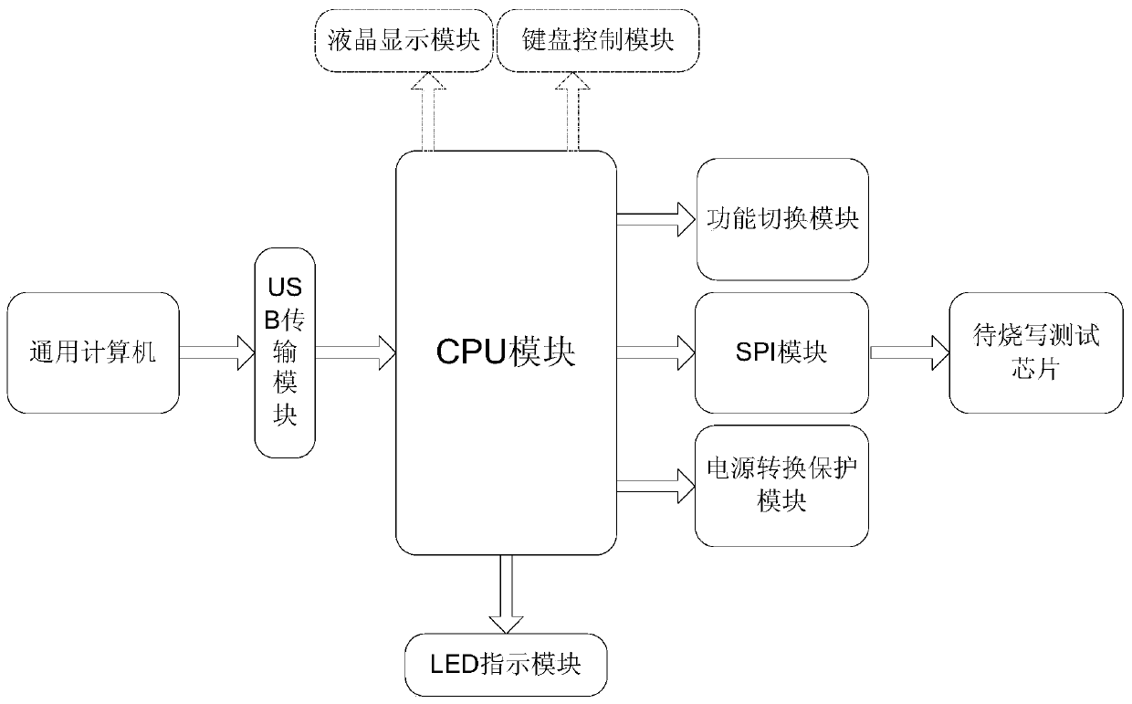
[0027] figure 1 It is a module schematic diagram of a programming test device for a programmable chip of the present invention, which includes a CPU module, an SPI module, a function switching module, a power conversion protection module, an LED indicator module, a liquid crystal display module, a keyboard control module, a USB transmission module, and a module to be burned. Write test chips, etc.

[0028] The CPU module is implemented by STM32F407VGT6 single-chip microco...


PUM


Abstract

The invention provides a chip programming test device, which comprises a CPU module, an SPI module, a power supply conversion protection module, a function switching module, an LED indication module,a USB transmission module and a keyboard control module, and also comprises two or more than two SPI interfaces to realize batch programming of a plurality of chips. According to the programmable chipprogramming test device provided by the invention, the chip does not need to be plugged and unplugged repeatedly; manual operation steps are simplified, computer does not need to be used, the original programmer is completely replaced; programming and testing programs can be automatically carried out by connecting a power supply; a serial port or a parallel port is not needed to simulate SPI communication, the SPI interface is directly used for programming the chip, the highest speed can reach 20 Mbps, meanwhile, 17 chips can be supported to perform programming tests at the same time, the programming efficiency is greatly improved, and the device is suitable for batch production tests.

Description

technical field [0001] The invention relates to the field of single-chip microcomputer development, in particular to a programming and testing device for a programmable chip. Background technique [0002] At present, in the field of single-chip microcomputer development, the following methods are generally adopted: one is the program burner method, and the other is the serial port / parallel port SPI simulation programming method. [0003] The program programmer method needs to use a separate programmer. When the source program needs to be modified, the single-chip microcomputer chip needs to be pulled out from the target board, and then the updated target code is re-solidified into the single-chip microcomputer chip. In this process, It is often necessary to repeatedly plug and unplug the chip, which is cumbersome to operate, which affects the life of the chip, and the program writer is generally expensive and the production cost is high. [0004] The serial port / parallel po...

Claims


Application Information

Patent Timeline
Patent Type & Authority Applications(China)
IPC IPC(8): G06F11/36G06F8/20
CPCG06F8/20G06F11/3672
Inventor 孙寿勇钟永铎丛珊珊尹江华
Owner QI AUTOMOTIVE CO LTD
Why Eureka
Try Eureka