Micro LED chip and display panel

A LED chip and miniature technology, applied in the direction of electrical components, electrical solid devices, circuits, etc., can solve the problems of difficult transfer and increase the difficulty of mass transfer, so as to avoid poor electrical contact, prevent electrical contact area from being too small, Improving the effect of misregistration

Active Publication Date: 2019-07-19
CHENGDU VISTAR OPTEOLECTRONICS CO LTD
View PDF7 Cites 13 Cited by
  • Summary
  • Abstract
  • Description
  • Claims
  • Application Information

AI Technical Summary

Problems solved by technology

In view of the relatively small size of micro-LED chips, it is not easy to realize the transfer in all assembly processes,

Method used


Image

  • Micro LED chip and display panel
  • Micro LED chip and display panel
  • Micro LED chip and display panel

Examples


Embodiment Construction

[0043] The technical solutions of the present invention will be further described below in conjunction with the accompanying drawings and through specific implementation methods. It should be understood that the specific embodiments described here are only used to explain the present invention, but not to limit the present invention. In addition, it should be noted that, for the convenience of description, only some structures related to the present invention are shown in the drawings but not all structures.

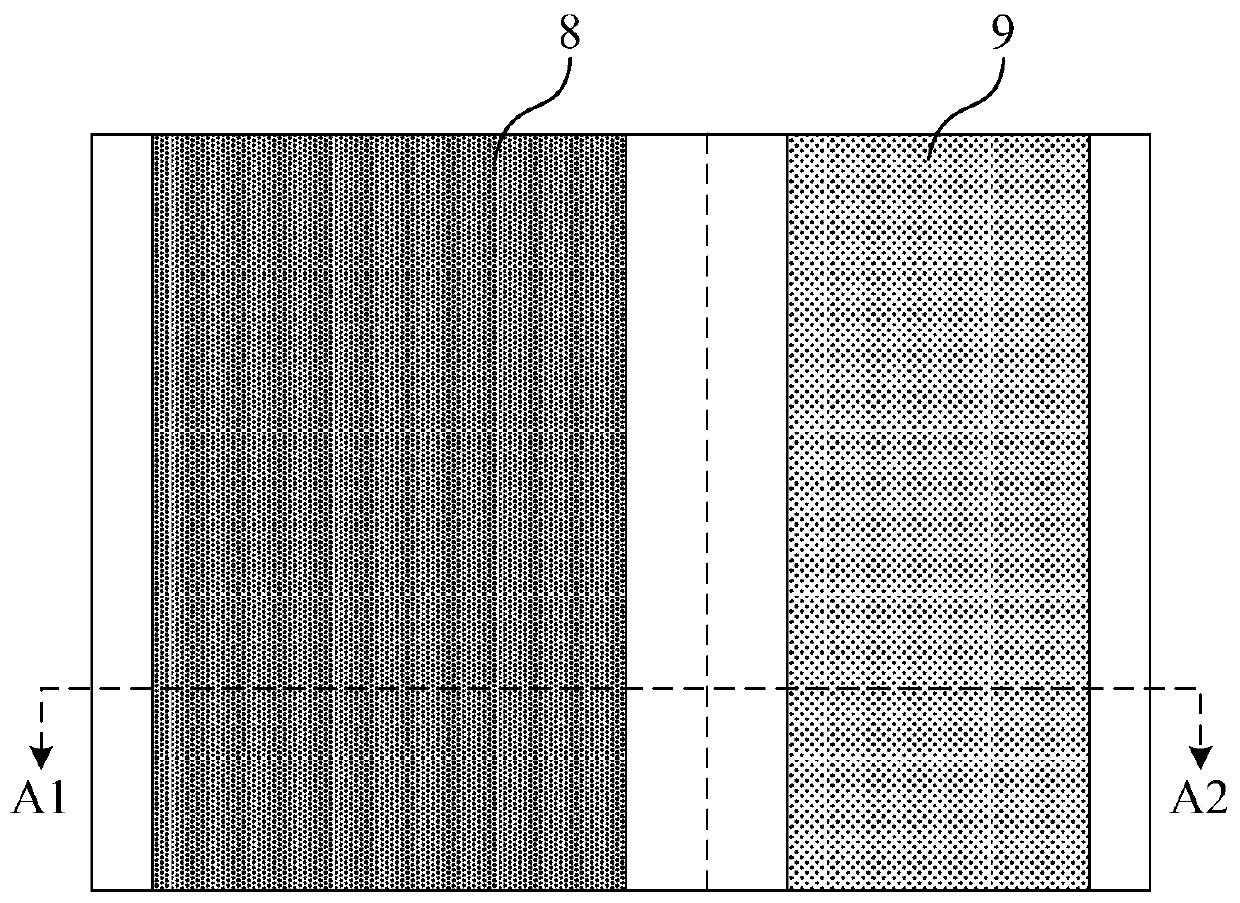
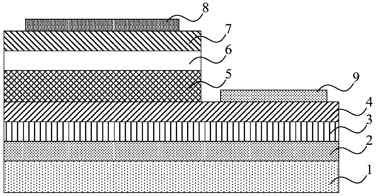
[0044] figure 1 It is a top view structural schematic diagram of an existing micro-LED chip; figure 2 for figure 1 Schematic diagram of the cross-sectional structure along the A1-A2 direction. Such as figure 1 and figure 2 As shown, the micro LED chip includes a substrate 1, a nucleation layer 2, a non-doped GaN layer 3, an n-type GaN layer 4, a multi-quantum well layer 5, an electron blocking layer 6 and a p-type GaN layer 7 stacked in sequence, Among them, part...


PUM


Abstract

The invention discloses a micro LED chip and a display panel. The micro LED chip comprises a substrate, a light emitting layer group positioned on the substrate, a first electrode and a second electrode, wherein the light emitting layer group at least comprises a first type semiconductor layer, a light emitting layer and a second type semiconductor layer which are arranged in a stacked mode; the first electrode and the second electrode are located on one side, far away from the substrate, of the light emitting layer group; the first electrode is electrically connected with the first type semiconductor layer; the second electrode is electrically connected with the second type semiconductor layer, wherein the first electrode is an annular electrode; the pattern of the outer edge and the pattern of the inner edge of the first electrode are the same; and the second electrode is located in the middle of a region surrounded by the inner edge of the first electrode. According to the embodiments of the invention, the electrode structure of the micro LED chip is improved, so that the difficulty of huge transfer of the micro LED chip is lowered.

Description

technical field [0001] Embodiments of the present invention relate to the field of micro LED display technology, in particular to a micro LED chip and a display panel. Background technique [0002] Light Emitting Diodes (LEDs) are widely used in technical fields such as lighting and display due to their advantages of small size, low power, long service life, high brightness and active light emission. Micro LED, also known as micro LED, mLED or μLED, is a new type of flat panel display technology. The micro LED display has an LED array of individual pixel elements. Compared with the widely used liquid crystal display, the micro LED display has a better contrast ratio. , Faster response speed, lower energy consumption. [0003] Since micro-LEDs are manufactured individually in the form of chips, a huge number of micro-LED chips need to be transferred to the backplane during the process of manufacturing a display device. At present, the mass transfer methods of micro-LED chip...

Claims


Application Information

Patent Timeline
IPC IPC(8): H01L33/38H01L27/15
CPCH01L27/156H01L33/38
Inventor 李庆韦冬邢汝博
Owner CHENGDU VISTAR OPTEOLECTRONICS CO LTD
Why Eureka
Try Eureka