
Method for forming a semiconductor device and semiconductor device

A semiconductor and device technology, applied in the formation method of semiconductor devices and the field of semiconductor devices, can solve the problems of large parasitic capacitance and reduce the AC performance of devices, and achieve the effects of small parasitic capacitance, improved AC performance and low resistance

Active Publication Date: 2022-03-29
SEMICON MFG INT (SHANGHAI) CORP +1
View PDF5 Cites 0 Cited by
  • Summary
  • Abstract
  • Description
  • Claims
  • Application Information

AI Technical Summary

Problems solved by technology

If the boron doping concentration is too high, it will lead to large parasitic capacitance
This degrades the AC performance of the device

Method used


Image

  • Method for forming a semiconductor device and semiconductor device
  • Method for forming a semiconductor device and semiconductor device
  • Method for forming a semiconductor device and semiconductor device

Examples


Embodiment Construction

[0045] The present invention is described below based on examples, but the present invention is not limited to these examples. In the following detailed description of the invention, some specific details are set forth in detail. The present invention can be fully understood by those skilled in the art without the description of these detailed parts. In order not to obscure the essence of the present invention, well-known methods, procedures, procedures, components and circuits have not been described in detail. Additionally, those of ordinary skill in the art will appreciate that the drawings provided herein are for illustrative purposes and are not necessarily drawn to scale.

[0046] Unless the context clearly requires, throughout the specification and claims, "comprises", "comprises" and similar words should be interpreted in an inclusive sense rather than an exclusive or exhaustive meaning; that is, "including but not limited to" meaning. In the description of the pres...


PUM

PropertyMeasurementUnit
thicknessaaaaaaaaaa
thicknessaaaaaaaaaa

Abstract

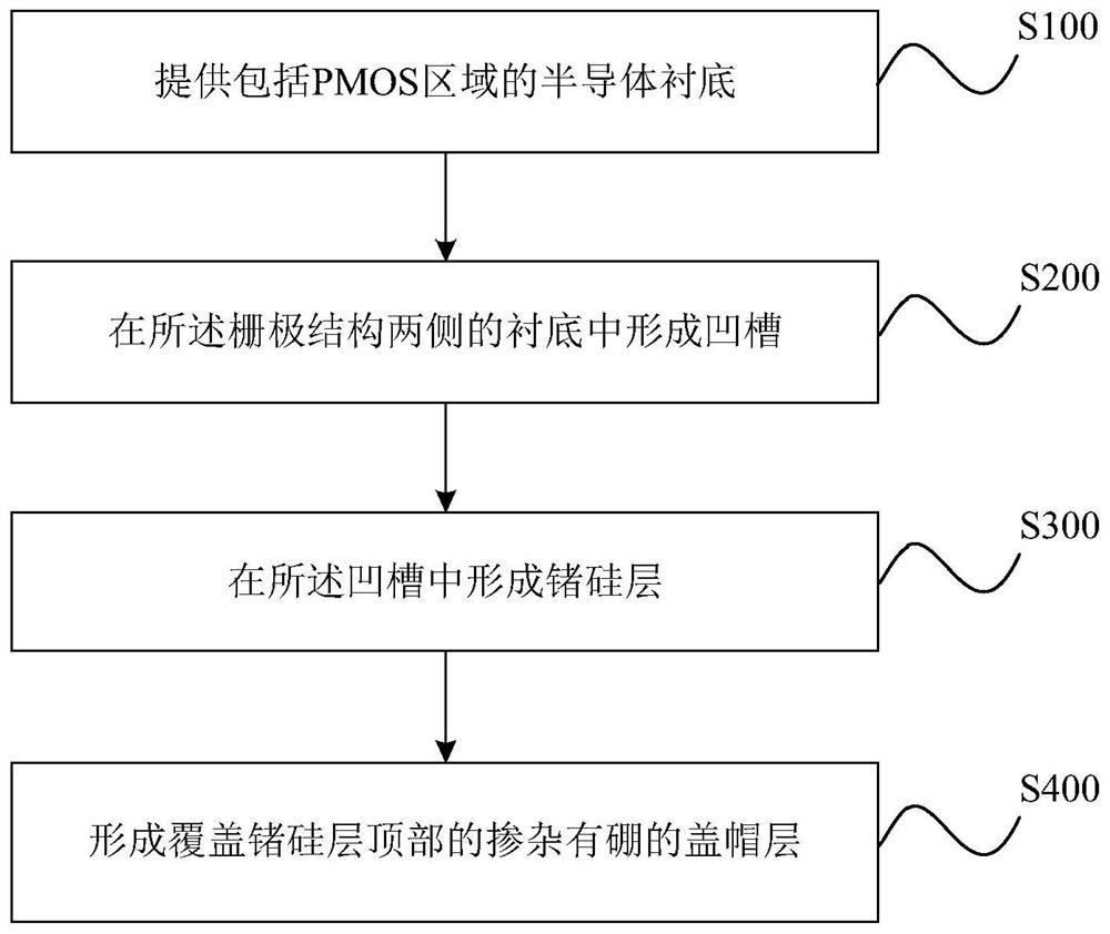
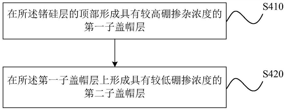
The invention discloses a method for forming a semiconductor device and the semiconductor device. The technical solution of the embodiment of the present invention controls the boron doping concentration of the cap layer covering the germanium-silicon layer during the formation of the semiconductor device, so that the boron doping concentration of the cap layer near the top of the germanium-silicon layer is greater than that of the region far away from the top of the germanium-silicon layer. The boron doping concentration of the region. As a result, the boron concentration at the bottom of the capping layer is higher, which has lower resistance, and improves the DC performance of the PMOS device. At the same time, the overall boron doping concentration of the capping layer remains low, so that it can have a small parasitic capacitance and improve the AC performance of the PMOS device.

Description

technical field [0001] The invention relates to semiconductor manufacturing technology, in particular to a method for forming a semiconductor device and the semiconductor device. Background technique [0002] When the critical dimension of the semiconductor manufacturing process reaches below 90nm, stress engineering (Stress Engineering) is widely used to improve the carrier mobility in the channel region of the semiconductor device. In the prior art, grooves are made in the source / drain region of PMOS (Positivechannel Metal Oxide Semiconductor, P-channel Metal Oxide Semiconductor) devices and filled to form an embedded silicon germanium (SiGe) layer to introduce compressive strain to the channel. , thereby increasing the mobility of holes in PMOS devices. [0003] In the process of forming the source / drain region using the SiGe layer, a cap layer (caplayer) needs to be formed on the SiGe layer. The capping layer is used to protect the silicon germanium layer, and is subse...

Claims


Application Information

Patent Timeline
Patent Type & Authority Patents(China)
IPC IPC(8): H01L21/336H01L29/78
CPCH01L29/66636H01L29/78
Inventor 刘震宇
Owner SEMICON MFG INT (SHANGHAI) CORP
Learn More