A lateral junction gate bipolar transistor and its manufacturing method

A bipolar transistor and junction gate technology, applied in semiconductor/solid-state device manufacturing, semiconductor devices, electrical components, etc., can solve the problems of high process difficulty and unstable devices, and achieve high carrier density, easy integration, The effect of enhancing stability

Active Publication Date: 2021-06-18
XIDIAN UNIV
View PDF8 Cites 0 Cited by
  • Summary
  • Abstract
  • Description
  • Claims
  • Application Information

AI Technical Summary

Problems solved by technology

At present, the process of LIGBT devices with wide bandgap semiconductor materials is relatively difficult, and the device may not be stable due to the latch-up effect

Method used


Image

  • A lateral junction gate bipolar transistor and its manufacturing method

Examples


Embodiment Construction

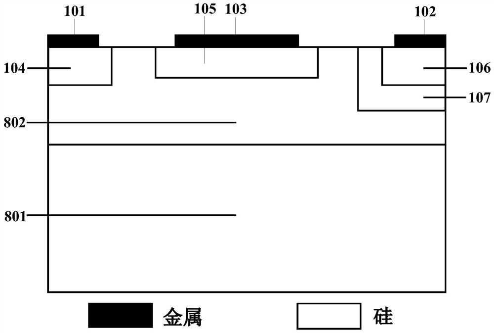
[0034] The present invention will be described below by taking an N-channel LJGBT as an example in conjunction with the accompanying drawings.

[0035] like figure 1 As shown, this embodiment includes:

[0036] P-type substrate 801 of wide bandgap semiconductor material;

[0037] N-type epitaxial layer 802 of wide bandgap semiconductor material formed on the upper surface of P-type substrate 801;

[0038] An N-type buffer region 107 formed in the upper right end region of the N-type epitaxial layer 802, and a P-type drain region 106 formed inside the N-type buffer region 107;

[0039] N-type source region 104 formed in the upper left end region of N-type epitaxial layer 802;

[0040] A P-type junction region 105 formed in the central region above the N-type epitaxial layer 802;

[0041] The source 101 is located on the upper surface of the N-type source region 104;

[0042] The drain 102 is located on the upper surface of the P-type drain region 106;

[0043] The gate 10...


PUM


Abstract

The invention provides a lateral junction gate bipolar transistor (LJGBT) and a manufacturing method thereof. The LJGBT device is based on the LIGBT structure, using a junction gate instead of an insulated gate, and its gate structure is similar to the PN junction gate structure of a conventional JFET, while the rest is similar to the conventional LIGBT structure. Compared with LIGBT, there is no parasitic NPN transistor structure in the LJGBT device structure, which is beneficial to eliminate the latch-up effect and enhance the stability of the device; complexity, solve the oxidation problem of wide bandgap semiconductor materials, and can also retain the advantages of voltage-controlled devices, that is, high input impedance. The LJGBT device is especially suitable for the field of low voltage and high current.

Description

technical field [0001] The invention relates to the field of power semiconductor devices, in particular to a lateral gate-controlled bipolar transistor. Background technique [0002] Power semiconductor devices refer to high-power electronic devices mainly used in power conversion and control circuits of power equipment. With the rapid development of power electronics technology, power semiconductor devices have been widely used in modern industrial control and national defense equipment. [0003] Lateral insulated gate bipolar transistor (LIGBT, Lateralinsulated gate bipolartransistor) is a very suitable power device for high-voltage power supply IC (HVIC) because it combines high input impedance and bipolar current conduction, while lateral devices are easy to integrate, and its The process can be compatible with the process of traditional complementary MOS (CMOS) chips. In recent years, the optimization of the characteristics of LIGBT devices is mainly to study LIGBT de...

Claims


Application Information

Patent Timeline
Patent Type & Authority Patents(China)
IPC IPC(8): H01L29/739H01L29/423H01L29/06H01L21/336
CPCH01L29/0611H01L29/423H01L29/66325H01L29/739
Inventor 段宝兴孙李诚王彦东杨银堂
Owner XIDIAN UNIV
Why Eureka
Try Eureka