PCB (Printed Circuit Board) manufacturing method with gold plating and gold melting processes

A technology of PCB board and manufacturing method, which is applied in the direction of printed circuit manufacturing, coating of non-metallic protective layer, secondary treatment of printed circuit, etc., can solve the problem that the lead cannot be completely removed from the short circuit lead, and the quality of the whole PCB board, so as to avoid short circuit Effect

Inactive Publication Date: 2019-07-23
ZHUHAI CHINA EAGLE ELECTRONIC CIRCTCUIS CO LTD
View PDF3 Cites 3 Cited by
  • Summary
  • Abstract
  • Description
  • Claims
  • Application Information

AI Technical Summary

Problems solved by technology

[0003] The purpose of the present invention is to solve the disadvantages of the existing PCB board processing process with gold plating and gold melting process, the lead wires cannot be completely removed and the gold infiltration at the lead wires leads to the short circuit lead PCB board quality, and to provide a gold plating and gold chemical process PCB board production method

Method used


Image

  • PCB (Printed Circuit Board) manufacturing method with gold plating and gold melting processes
  • PCB (Printed Circuit Board) manufacturing method with gold plating and gold melting processes

Examples


Embodiment Construction

[0022] In order to make the object, technical solution and advantages of the present invention clearer, the present invention will be further described in detail below in conjunction with the accompanying drawings and embodiments. It should be understood that the specific embodiments described here are only used to explain the present invention, not to limit the present invention.

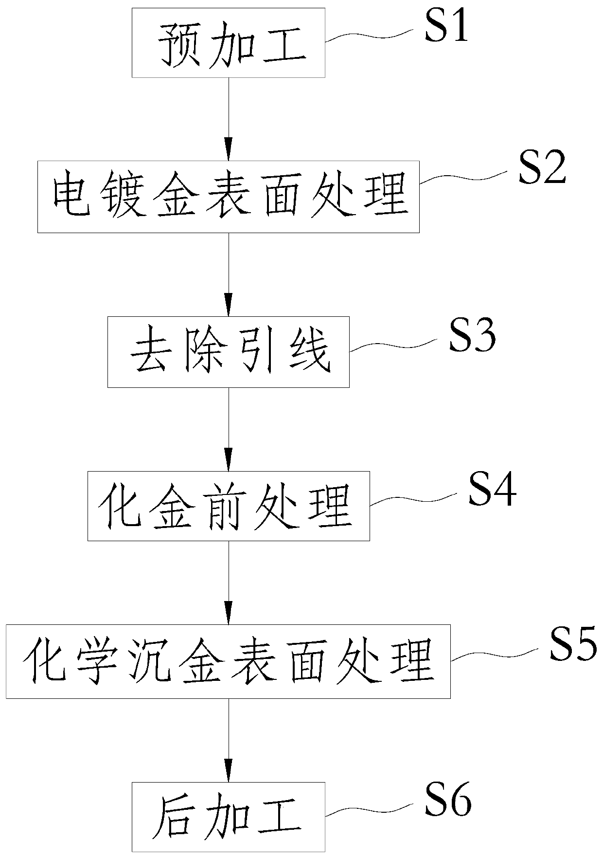
[0023] see figure 1 , is a process flow chart of a method for manufacturing a PCB with gold plating and gold plating processes provided by the present invention. Such as figure 1 Shown, for a kind of PCB board manufacturing method provided by the present invention with gold plating and gold chemical process, comprises the following steps:

[0024] S1: pre-processing to prepare a multilayer circuit board with outer layers of circuits. Among them, the preprocessing includes the steps of cutting, drilling, whole board electroplating, image transfer, pattern electroplating and pattern etching, as fo...


PUM


Abstract

The invention provides a PCB (Printed Circuit Board) manufacturing method with gold plating and gold melting processes, which comprises the following steps of: pre-processing to obtain a multi-layer circuit board with an outer-layer circuit; performing electrogilding surface treatment; removing the lead; pretreatment of gold melting: respectively carrying out oxidation resistance treatment and resistance welding on the multi-layer circuit board; carrying out chemical immersion gold surface treatment; and performing post-processing to obtain the PCB. According to the PCB manufacturing method with gold plating and gold melting processes, firstly, electrogilding surface treatment and lead removal are carried out on the multi-layer circuit board; then gold melting pretreatment is carried out;oxidation resistance treatment and resistance welding are carried out on the multi-layer circuit board; and then, chemical immersion gold surface treatment is carried out, according to the process flow, not only is the product quality of the gold plating area ensured, but also the product quality of the gold melting area is ensured, the problem of lead gold seepage during electrogilding surface treatment is more effectively solved, and meanwhile leads can be completely removed in the lead removal step.

Description

technical field [0001] The invention relates to the technical field of printed circuit board processing, in particular to a method for manufacturing a PCB board with gold-plating and gold-melting processes. Background technique [0002] With the continuous development of science and technology, the performance requirements for printed circuit boards are also getting higher and higher. Therefore, in order to meet the various electrical performance requirements of the PCB board, not only electroplating gold surface treatment is required during PCB board processing, but also chemical immersion gold surface treatment is required to meet the design requirements of the PCB board. And in the existing PCB board processing process with gold-plating and gold-melting process, all are to carry out gold-plating and gold-melting process again on the multi-layer circuit board that has made outer circuit and solder resist layer. However, the lead wires produced by pattern electroplating on...

Claims


Application Information

Patent Timeline
Patent Type & Authority Applications(China)
IPC IPC(8): H05K3/18H05K3/28
CPCH05K3/18H05K3/282
Inventor 黄生荣杨鹏飞邱成伟李小海王晓槟
Owner ZHUHAI CHINA EAGLE ELECTRONIC CIRCTCUIS CO LTD
Why Eureka
Try Eureka