
Processing method for PCB wire residues and printed circuit board

A treatment method and wire technology, applied in printed circuit, printed circuit manufacturing, chemical/electrolytic method to remove conductive materials, etc., can solve the problems of printed circuit board gold-infiltrated wire residue, wire gold-infiltrated, and film gaps, etc. , to achieve the effect of reducing production costs and avoiding delivery deadlines

Pending Publication Date: 2022-01-07
珠海杰赛科技有限公司 +2
View PDF4 Cites 0 Cited by
  • Summary
  • Abstract
  • Description
  • Claims
  • Application Information

AI Technical Summary

Problems solved by technology

[0003] In the prior art, when the printed circuit board is produced by the dry film cover wire method, there is a gap in the film due to the level difference of the circuit in the circuit board, and the wire will seep gold during the process of wire flash gold plating, and when the wire is etched , the gold-infiltrated wires cannot be etched by alkaline etching solution, which will result in residual gold-infiltrated wires on the printed circuit board

Method used


Image

  • Processing method for PCB wire residues and printed circuit board

Examples


Embodiment Construction

[0022] Embodiments of the present invention will be described in detail below, and examples of the embodiments are illustrated in the drawings, in which the same or similar reference numerals represent the same or similar elements or elements having the same or similar functions. The following is exemplary, and is intended to be illustrative of the invention, not to be construed as limiting the invention.

[0023] In the description of the present invention, it is to be understood that the orientation or positional relationship of the orientation, such as upper, lower, prior,,, left, right, etc., based on the orientation or positional relationship shown in the drawings, is only In order to facilitate the description of the invention and simplified description, rather than indicating or implying that the device or element must have a specific orientation, constructing and operating in a particular orientation, and thus is not to be construed as limiting the invention.

[0024] In t...


PUM


Abstract

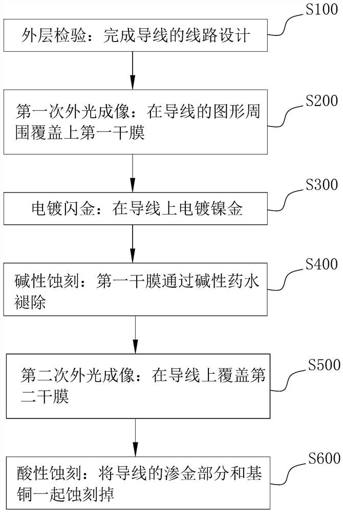
The invention discloses a processing method for PCB wire residues and a printed circuit board. The processing method for the PCB wire residues comprises the following steps of inspecting an outer layer to complete the line design of a wire; carrying out primary external light imaging, namely covering a first dry film around a pattern of the wire; electroplating flash gold, namely electroplating nickel gold on the wire; carrying out alkaline etching, namely removing the first dry film through alkaline liquid medicine; carrying out secondary external light imaging, namely covering a second dry film on the wire; and carrying out acid etching, namely etching off the gold infiltrating part of the wire and the base copper together, thereby removing the gold infiltrating wire residues on the printed circuit board, preventing product scrapping from influencing the delivery period of product production, and reducing the production cost.

Description

Technical field [0001] The present invention relates to printed circuit board manufacturing technology, and particularly relates to a method for processing residual PCB wires and printed circuit board. Background technique [0002] The printed circuit board as the base components of the electronic device, is a transmission carrier current, signals, plays an important role in the electronic device, so the printed circuit board of a higher quality requirements. [0003] In the prior art, the printed circuit board using the dry film method in the production of the wire cover, the circuit board having a wiring film height difference caused by voids, metal infiltration will lead wire during the flash gold plated, etched wire , infiltration of gold wire can not be etched alkali etching solution, leading to the printed circuit board will retentate remaining gold wire. Inventive content [0004] The present invention is intended to solve at least one of the technical problems present in...

Claims


Application Information

Patent Timeline
IPC IPC(8): H05K3/06
CPCH05K3/067
Inventor 蔡永伦张良昌冯涛唐培林
Owner 珠海杰赛科技有限公司
Learn More