Separation tool-based mask tape cutting method
A separate and tooling technology, applied in the secondary processing of printed circuits, electrical components, printed circuit manufacturing, etc., can solve the problems of discontinuous step sawtooth, difficult masking tape cutting, discontinuous rounded corners, etc., to improve cutting Efficiency, saving labor costs, and reducing losses
- Summary
- Abstract
- Description
- Claims
- Application Information
AI Technical Summary
Problems solved by technology
Method used
Image
Examples
Embodiment 1
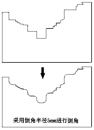
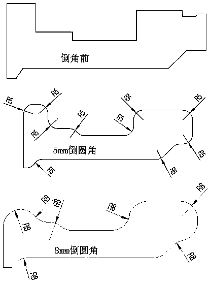
[0025] A masking tape cutting method based on separate tooling, such as figure 1 , figure 2 As shown, the irregular edge of the separate tooling is smoothed, and the irregular edge of the separate tooling forms a smooth arc with a radius of 5mm.
[0026] In the process of tooling separation design in the present invention, the actual PCB has a step-like sawtooth irregular shape, which has problems such as discontinuity or rounded corners embedded, and it is difficult to cut the masking tape when cutting by hand. The edge forms a smooth chamfering pattern; after smoothing the irregular edge of the separate tooling and then cutting the masking tape, the irregular edge of the separate tooling forms a smooth arc with a radius of 5mm, which is convenient for manual cutting. , which improves the cutting efficiency of the masking tape; on the other hand, it can ensure the masking effect of the masking tape cut by the separate tooling on the PCB mounting board.
Embodiment 2
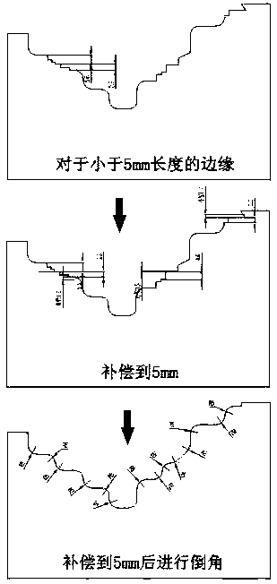
[0028] This embodiment is further optimized on the basis of embodiment 1, as figure 1 As shown, when the length at the edge is greater than 5mm, use a chamfering radius of 5mm for chamfering; as figure 2 As shown, when the length at the edge is less than 5mm, the edge length is compensated to 5mm, and then the chamfering radius is 5mm for chamfering.
[0029] The invention can handle separate tooling with different edge lengths. The smooth chamfering of the separate tooling ensures the smoothness of manual cutting and reduces the loss of the area of the separate tooling. The loss of area makes the masking effect of the masking tape on the PCB mounting board reach the target, so as to achieve the normal cutting level. The invention improves the work efficiency, reduces the loss in the cutting process, saves the labor cost, and has better practicability.
[0030] Other parts of this embodiment are the same as those of Embodiment 1, so details are not repeated here.
Embodiment 3
[0032] A masking tape cutting method based on separate tooling, such as Figure 5 shown, including the following steps:
[0033] Step 1: Draw a drawing of the separate tooling;
[0034](1) Draw a drawing of the separate tooling according to the shielding part of the PCB mounting board;
[0035] (2) Chamfer the edge of the separate tooling in the drawing: as figure 1 As shown, firstly, the edge of the separate tooling larger than 5mm in the drawing is chamfered for the first time with a radius of 5mm, so that the edge of the separate tooling larger than 5mm forms an arc with a radius of 5mm; figure 2 As shown, then the edge of the separate tooling less than 5mm in the drawing is compensated to 5mm; finally, the second chamfering with a radius of 5mm is performed on the edge after the compensation of the separate tooling in the drawing.
[0036] Step 2: Prepare separate tooling;
[0037] (1) Choose an aluminum plate with a thickness of 1mm-1.5mm as the preparation material ...
PUM
 Abstract
Description
Claims
Application Information
 - R&D
- Intellectual Property
- Life Sciences
- Materials
- Tech Scout
- Unparalleled Data Quality
- Higher Quality Content
- 60% Fewer Hallucinations
Browse by: Latest US Patents, China's latest patents, Technical Efficacy Thesaurus, Application Domain, Technology Topic, Popular Technical Reports.
© 2025 PatSnap. All rights reserved.Legal|Privacy policy|Modern Slavery Act Transparency Statement|Sitemap|About US| Contact US: help@patsnap.com


