
Manufacturing method of touch screen

A touch screen and flexible material layer technology, applied in the input/output process of data processing, instruments, inks, etc., can solve the problems of complex process steps, residual silver paste, high production costs, etc., to simplify the process and ensure cleanliness degree, to ensure the effect of zero-valent chemical valence state

Active Publication Date: 2021-11-05
SUZHOU LANPEI OPTOELECTRONICS TECH CO LTD
View PDF9 Cites 0 Cited by
  • Summary
  • Abstract
  • Description
  • Claims
  • Application Information

AI Technical Summary

Problems solved by technology

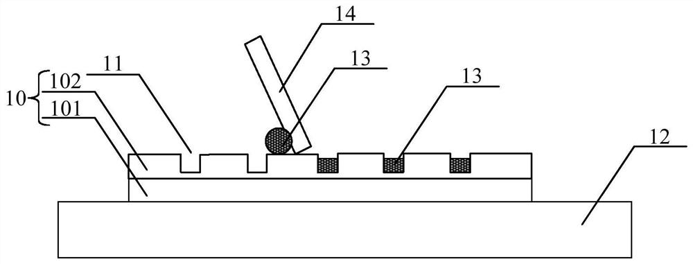
[0005] In view of the above-mentioned shortcomings of the prior art, the purpose of the present invention is to provide a method for preparing a touch screen, which is used to solve the problem that the flexible material layer may be caused by scraping silver paste on the upper surface of the flexible material layer in the prior art. There is silver paste residue on the upper surface, so the upper surface of the flexible material layer needs to be cleaned after the scraping is completed, and the silver paste can be sintered and solidified to form a conductive layer after cleaning, which makes the whole process steps more complicated and the production cost is higher problems, as well as the use of silver paste to make conductive layers, because silver paste is a noble metal, which leads to the problem of high cost

Method used


Image

  • Manufacturing method of touch screen
  • Manufacturing method of touch screen
  • Manufacturing method of touch screen

Examples


Embodiment Construction

[0100] Embodiments of the present invention are described below through specific examples, and those skilled in the art can easily understand other advantages and effects of the present invention from the content disclosed in this specification. The present invention can also be implemented or applied through other different specific implementation modes, and various modifications or changes can be made to the details in this specification based on different viewpoints and applications without departing from the spirit of the present invention.

[0101] see Figure 2 to Figure 17 . It should be noted that the diagrams provided in this embodiment are only schematically illustrating the basic concept of the present invention, although only the components related to the present invention are shown in the diagrams rather than the number, shape and Dimensional drawing, the type, quantity and proportion of each component can be changed arbitrarily during actual implementation, and ...


PUM

PropertyMeasurementUnit
thicknessaaaaaaaaaa
particle diameteraaaaaaaaaa

Abstract

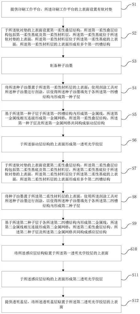
The invention provides a method for preparing a touch screen, comprising the following steps: providing a printing work platform provided with a soft pad; preparing seed ink; using a scraping tool on the soft pad to scrape the seed ink on each first Forming a first seed layer in the groove structure; forming a first metal line in the first groove structure based on the first seed layer; forming a first transparent optical adhesive layer on the upper surface of the driving layer structure; using a scraper on the soft pad The coating tool scrapes the seed ink to form a second seed layer in each second groove structure; forms a second metal line in each second groove structure based on the second seed layer; attaches the sensing layer structure to the first transparent The upper surface of the optical adhesive layer; forming a second transparent optical adhesive layer on the upper surface of the sensing layer structure; providing a transparent cover layer, and pasting the transparent cover layer on the upper surface of the second transparent optical adhesive layer. The invention does not need additional steps of pre-curing and cleaning, thereby simplifying the technological process and reducing the production cost.

Description

technical field [0001] The invention belongs to the field of touch technology, in particular to a method for preparing a touch screen. Background technique [0002] The touch screen generally has a metal grid to form a channel and has functions. Metal grids are mostly regular graphics, such as rectangles, rhombuses or hexagons, etc. The metal grid in the existing touch screen is generally obtained by forming a conductive layer in the groove structure of the flexible material layer, and the obtained metal grid is connected to the processing chip through a flexible circuit board (FPC). In the prior art, methods for forming a conductive layer such as figure 1 As shown, generally, the flexible laminated structure 10 including the flexible substrate 101 and the flexible material layer 102 is placed on the upper surface of a printing platform 12, and the silver paste 13 is dripped on the upper surface of the flexible material layer 102 using a scraper 14 Scraping the silver pas...

Claims


Application Information

Patent Timeline
Patent Type & Authority Patents(China)
IPC IPC(8): G06F3/041C09D11/03
CPCC09D11/03G06F3/041G06F2203/04103
Inventor 谢自民冯波郭向阳陈春明平财明林涛
Owner SUZHOU LANPEI OPTOELECTRONICS TECH CO LTD
Learn More