Switching converter and control method thereof

A technology of switching converters and control methods, applied in control/regulation systems, DC power input conversion to DC power output, instruments, etc., can solve the problem of large conduction loss, difficulty in large current output and high frequency, inductor L1 Long demagnetization time and other problems

Active Publication Date: 2019-08-02
MORNSUN GUANGZHOU SCI & TECH
View PDF3 Cites 2 Cited by
  • Summary
  • Abstract
  • Description
  • Claims
  • Application Information

AI Technical Summary

Problems solved by technology

[0005] In view of the technical defects of the existing reverse polarity circuit, the present invention proposes a switching converter circuit and its control method. The circuit works in the discontinuous mode to reduce the effective value of the current and solve the problem of large conduction loss; all switches The tube realizes ZVS turn-on, when the absolute value of the intermittent mode and the ratio of input and output voltage is greater than 2, it solves the problem that the demagnetization time of the inductor L1 is too long, and it is difficult to output large current and high frequency

Method used


Image

  • Switching converter and control method thereof
  • Switching converter and control method thereof
  • Switching converter and control method thereof

Examples


no. 1 example

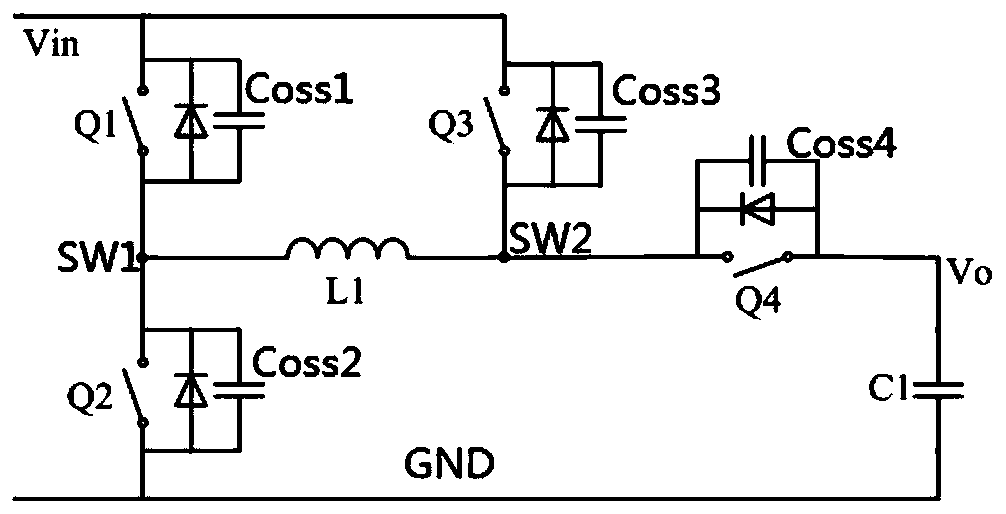
[0064] image 3 It is the schematic circuit diagram of the first embodiment of the present invention. Including input power supply positive Vin, output voltage negative Vo, power supply common ground, MOS transistor Q1, MOS transistor Q2, MOS transistor Q3, MOS transistor Q4, inductor L1 and capacitor C1; the drain of MOS transistor Q1 and the drain of MOS transistor Q3 The drain is connected to the positive Vin of the input power supply, the source of the MOS transistor Q1 and the drain of the MOS transistor Q2 are connected to one end of the inductor L1, the source of the MOS transistor Q3 and the drain of the MOS transistor Q4 are connected to the other end of the inductor L1 At one end, the source of the MOS transistor Q4 is connected to one end of the capacitor C1, and the source of the MOS transistor Q2 and the other end of the capacitor C1 are connected to the power common ground GND.

[0065] image 3 Coss1, Coss2, Coss3 and Coss4 are the output capacitances of MOS t...

no. 2 example

[0101] Figure 7 It is the schematic circuit diagram of the second embodiment of the present invention. On the basis of the first embodiment, the MOS transistor Q1 is replaced by a diode D1, the cathode of the diode D1 is connected to the drain of the MOS transistor Q3 and the positive input power Vin, and the anode of the diode D1 is connected to the drain of the MOS transistor Q2 and the inductance one end of L1.

[0102] The time for the diode D1 to flow current is relatively short. Compared with the MOS tube solution, the conduction loss will not increase too much, but it saves a floating drive, reduces the drive loss, simplifies the drive circuit, and is suitable for small and medium current output. Scenes.

[0103] In this embodiment, the absolute value of the ratio of the input-to-output voltage is greater than 2, and a better implementation effect can also be obtained. For a switching converter with a Vin voltage of 75V, a Vo voltage of negative 12V, an inductor L1 o...


PUM


Abstract

The invention discloses a switching converter and a control method thereof. The switching converter comprises a positive input power supply, a negative output voltage, a power supply common ground, aswitch transistor Q1, a switch transistor Q2, a switch transistor Q3, a switch transistor Q4, an inductor L1 and a capacitor C1, wherein the drain electrode of the switch transistor Q1 and the drain electrode of the switch transistor Q3 are connected to the positive input power supply, the source electrode of the switch transistor Q1 and the drain electrode of the switch transistor Q2 are connected to one end of the inductor L1, the source electrode of the switch transistor Q3 and the drain electrode of the switch transistor Q4 are connected to the other end of the inductor L1, the source electrode of the switch transistor Q4 is connected to one end of the capacitor C1, and the source electrode of the switch transistor Q2 and other end of the capacitor C1 are connected to the power supplycommon ground. According to the invention, the input voltage and the output voltage are opposite in polarity, all switch transistors ZVSs are turned on, and the efficiency is high; fast demagnetization of the inductor L1 can be realized when the absolute value of the ratio of the input and output voltage is great, the current waveform of the inductor L1 is changed from triangular into quadrilateral, and the high-frequency efficient operation of the switching converter is realized.

Description

technical field [0001] The invention relates to a switching power supply, in particular to a switching converter circuit and a control method thereof. Background technique [0002] figure 1 It is a traditional Buck_Boost circuit. When the circuit works in discontinuous mode, the effective value of the current is relatively large, and the MOS tube Q1 is hard-switched, and the conduction loss of D1 is large. [0003] figure 2 It is a CUK circuit, which is a fourth-order or even higher-order circuit. The dynamic process is complex, and the output is easy to overshoot. The circuit works in discontinuous mode. [0004] Both the traditional Buck_Boost circuit and the CUK circuit are reverse polarity circuits, and the input and output voltages are reversed. However, there are problems that the effective value of the current is large and the conduction loss is too large when the circuit works in discontinuous mode; the MOS transistor Q1 is hard-switched, and the switching loss i...

Claims


Application Information

Patent Timeline
Patent Type & Authority Applications(China)
IPC IPC(8): H02M3/158
CPCH02M3/158H02M1/0058Y02B70/10
Inventor 卢鹏飞
Owner MORNSUN GUANGZHOU SCI & TECH
Why Eureka
Try Eureka