
A chip adsorption device and chip bonding system

A technology for adsorption devices and chips, which is applied in the manufacture of electrical components, circuits, semiconductors/solid-state devices, etc., can solve the problems of reduced yield, increased cost, and decreased work efficiency, and can improve the moving speed and placement speed and reduce the accuracy Requirements, the effect of improving work efficiency

Active Publication Date: 2021-06-04
SHANGHAI MICRO ELECTRONICS EQUIP (GRP) CO LTD
View PDF6 Cites 0 Cited by
  • Summary
  • Abstract
  • Description
  • Claims
  • Application Information

AI Technical Summary

Problems solved by technology

In the operation of the chip, the single-hole suction cup installed on the stage is uniquely designed according to the size of the chip. When the size of the chip changes, the stage needs to be replaced synchronously, resulting in a decrease in the utilization rate of the stage, prolonging the production operation time, and increasing the cost; in addition In addition, the single-hole suction cup has a large aperture. In order to facilitate vacuum adsorption, the chip must be placed at the center of the aperture. The accuracy of the chip placement is very high. Usually, in order to ensure the accuracy of the chip position, the moving speed of the bonding hand before placing the chip needs to be reduced, resulting in a decrease in work efficiency and a decrease in productivity

Method used


Image

  • A chip adsorption device and chip bonding system
  • A chip adsorption device and chip bonding system
  • A chip adsorption device and chip bonding system

Examples


Embodiment 1

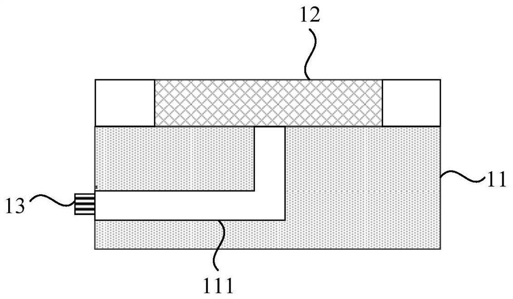
[0032] figure 1 It is a schematic structural diagram of a chip adsorption device provided in Embodiment 1 of the present invention, refer to figure 1 , the chip adsorption device includes: a base plate 11, a porous ceramic chuck 12 positioned on the base plate, and a vacuum source 13; the inside of the base plate 11 is provided with a first air guide channel 111 that is in contact with the non-adsorption surface of the porous ceramic chuck 12, the second A first end of an air guide channel 111 communicates with the air holes exposed on the non-adsorption surface of the porous ceramic suction cup 12 , and a second end of the first air guide channel 111 communicates with the vacuum air source 13 .

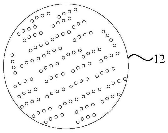
[0033] figure 2 It is a structural schematic diagram of a porous ceramic sucker provided in Embodiment 1 of the present invention, refer to figure 2 , the porous ceramic chuck 12 contains air holes with a pore size on the order of microns, and the air holes communicate with each ...

Embodiment 2

[0038] The traditional vacuum control method usually adopts the method of vacuuming all the pores of the suction cup when the adsorption device absorbs the chip. This vacuum control method can easily cause the suction cup to absorb dust and impurities in the area not covered by the chip, which affects the adsorption of other larger-sized chips. As a result, the service life of the chip adsorption device is reduced, and the difficulty of cleaning is also increased.

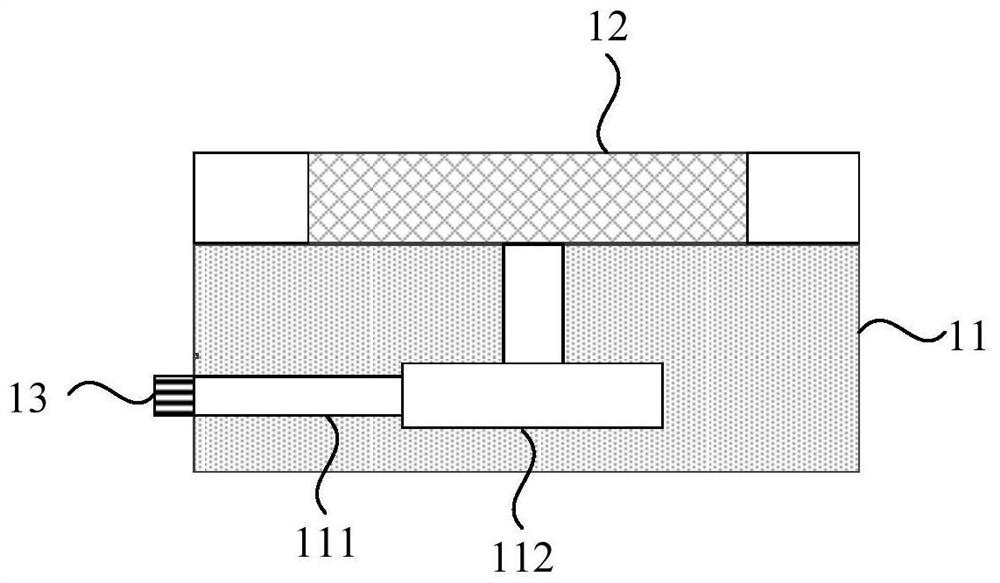
[0039] Figure 4 It is a schematic structural diagram of a chip adsorption device provided in Embodiment 2 of the present invention, refer to Figure 4, the vacuum adsorption device comprises a base plate 11, a porous ceramic chuck 12 positioned on the base plate and a vacuum source 13; the inside of the base plate 11 is provided with a first air guide channel 111 in contact with the non-adsorption surface of the porous ceramic chuck 12, the first The first end of the air guide channel 111 communicates with the ai...

Embodiment 3

[0049] Figure 11 It is a schematic structural diagram of a chip bonding system provided in Embodiment 3 of the present invention, refer to Figure 11 , the chip bonding system includes a bonding hand 100 , a stage 200 , a bonding stage 300 and at least one chip adsorption device 400 according to any one of the previous embodiments arranged on the stage 200 . Wherein, the chip 500 is adsorbed on the stage 200 by the chip adsorption device 400 .

[0050] Refer below figure 1 and Figure 11 The working process of the chip bonding system is introduced: first, the stage 200 moves to the transfer position, and the picker (not shown in the figure) places the chip 500 on the chip adsorption device 400 of the stage 200, and the chip adsorption device 400 The vacuum air source 13 in the vacuum chamber is activated, and the porous ceramic chuck 12 is provided with a vacuum through the second air guide channel 111, and the porous ceramic chuck 12 is equipped with a suction force under...


PUM

PropertyMeasurementUnit
pore sizeaaaaaaaaaa

Abstract

The invention discloses a chip adsorption device and a chip bonding system. The chip adsorption device comprises: a substrate, a porous ceramic suction cup positioned on the substrate, and a vacuum air source; the interior of the substrate is provided with a first air guide channel in contact with the non-adsorption surface of the porous ceramic suction cup, the The first end of the first air guide channel communicates with the air holes exposed on the non-adsorption surface of the porous ceramic suction cup, and the second end of the first air guide channel communicates with a vacuum air source. The embodiment of the present invention solves the problem that the single-hole suction cup can only absorb chips of a specific size, and when the size of the chip changes, the carrier needs to be replaced accordingly, realizing effective adsorption of chips of different sizes, improving the utilization rate of the carrier and the chip The efficiency of the bonding system; and it can reduce the accuracy requirements of the chip placement position, thereby increasing the moving speed and placement speed of the pick-up hand and the bonding hand, and improving work efficiency.

Description

technical field [0001] Embodiments of the present invention relate to semiconductor technology, and in particular to a chip adsorption device and a chip bonding system. Background technique [0002] In the process of semiconductor packaging, semiconductor chips are often mounted on substrates or other carriers for processing. Chip operation is a key process in electronic packaging, including chip jacking, stripping, pick-up and placement, and other operations. The device of the chip is a carrier. In order to avoid the position of the chip moving during the movement of the carrier and cause the picking error of the bonding hand, a suction cup is installed on the carrier to fix the chip. The current mature sucker is an ordinary single-hole sucker. The hole diameter of the sucker is millimeter-level and uniquely designed according to the size of the chip. It can only absorb chips of certain sizes. When the size of the bonded chip changes, the carrier needs to be replaced accord...

Claims


Application Information

Patent Timeline
Patent Type & Authority Patents(China)
IPC IPC(8): H01L21/683H01L21/67
CPCH01L21/67092H01L21/6838
Inventor 程静郭耸
Owner SHANGHAI MICRO ELECTRONICS EQUIP (GRP) CO LTD
Learn More