Supercharge Your Innovation With Domain-Expert AI Agents!

Dual optical path laser processing device and method for wafer scribing

A laser processing and optical path technology, applied in laser welding equipment, metal processing equipment, manufacturing tools, etc., can solve the problems of complex adjustment and low efficiency, and achieve the effect of ensuring the processing effect.

Pending Publication Date: 2019-08-09
ZHEJIANG HOLY LASER TECH CO LTD
View PDF0 Cites 3 Cited by
  • Summary
  • Abstract
  • Description
  • Claims
  • Application Information

AI Technical Summary

Problems solved by technology

[0003] At the same time, due to the strong demand in the field of consumer electronics, it is increasing at a rate of more than 20% every year; as we all know, laser scribing equipment is the basis for the development of the wafer industry in the field of consumer electronics. The degree of precision is inseparable. The fully automatic laser processing device based on wafer scribing is a particularly important link in the wafer manufacturing process. At present, wafer scribing mainly relies on a single optical path to act on the wafer, and applies it through a single optical path that emits different energies before and after. For the wafer, the efficiency is low, and the adjustment is complicated

Method used


Image

  • Dual optical path laser processing device and method for wafer scribing
  • Dual optical path laser processing device and method for wafer scribing

Examples


specific Embodiment approach

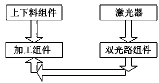
[0023] Such as figure 1 As shown, the wafer dicing processing device in this embodiment includes four parts: loading and unloading components, lasers, dual optical path components and processing components, wherein the loading and unloading components and processing components all adopt the existing technology, and the beam processing components include A moving processing table, the processing table is a quartz adsorption carrier.

[0024] The fully automatic laser processing device for wafer scribing provided by the present invention transmits the wafer to be processed to the processing table of the processing assembly through the loading and unloading assembly, and then turns on the laser and the dual optical path assembly for processing.

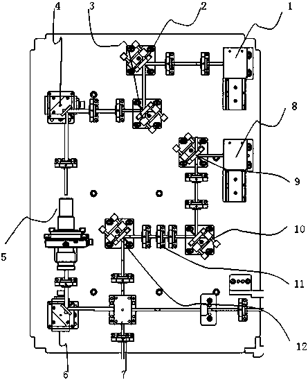
[0025] Such as figure 2 As shown, the dual optical path assembly includes an optical gate A1, an optical gate B8, a beam expander 5, a polarizing beam splitter 7, and a half-wavelength plate 11; the laser light generated by the laser p...


PUM


Abstract

The invention relates to a dual optical path laser processing device and method for wafer scribing. The dual optical path laser processing device comprises a laser device and a dual optical path assembly, the dual optical path assembly comprises an optical gate A, an optical gate B, a beam expanding mirror, a polarizing spectroscope, and a half wavelength plate; lasers generated by the laser device form an optical path A and an optical path B; the optical path A enters the beam expanding mirror after the optical path A is reflected by an optical path A reflecting mirror, and after the beam expanding mirror expands an optical beam, the optical path A enters the polarizing spectroscope after passing an optical path A reflecting mirror again; the optical path B reaches the half wavelength plate after the optical path B is reflected by an optical path B reflecting mirror, and B enters the polarizing spectroscope after is adjusted and after passing an optical path B reflecting mirror again;and the lasers emitted by the polarizing spectroscope are focused on a wafer to be processed. According to the dual optical path laser processing device and method for the wafer scribing, laser spotscan be dynamically adjusted of the deflected optical beam of the optical path A through the beam expanding mirror to meet the complex processing requirements, laser device energy can be dynamically adjusted after the optical beam deflected by the optical path B passes through the half wavelength plate, and thus the processing effect is ensured.

Description

technical field [0001] The invention relates to the technical field of wafer dicing processing, in particular to a dual-optical-path laser processing device and method for wafer dicing. Background technique [0002] The most critical technology for wafer processing is laser scribing technology. In recent years, due to the increasingly fierce competition in the industry, the efficiency and accuracy of scribing equipment are increasingly demanding. The cutting process has changed from the previous 30um to the current 10um. , The single-chip production capacity has increased by more than 50% compared with the previous one, the luminous brightness has increased by more than 20% compared with the previous one, and the chip size has been upgraded to a smaller 03*05mil. [0003] At the same time, due to the strong demand in the field of consumer electronics, it is increasing at a rate of more than 20% every year; as we all know, laser scribing equipment is the basis for the develop...

Claims


Application Information

Patent Timeline
Patent Type & Authority Applications(China)
IPC IPC(8): B23K26/362B23K26/06B23K26/067B23K26/70
CPCB23K26/362B23K26/0673B23K26/0643B23K26/702
Inventor 邵西河卢巍
Owner ZHEJIANG HOLY LASER TECH CO LTD
Features
  • R&D
  • Intellectual Property
  • Life Sciences
  • Materials
  • Tech Scout
  • Unparalleled Data Quality
  • Higher Quality Content
  • 60% Fewer Hallucinations
Learn More