
Flash memory programming system and method

A memory and writer technology, applied in instruments, electrical digital data processing, computing, etc., can solve the problems of programming efficiency, time-consuming, etc., and achieve the goal of shortening programming time, reducing communication time, and improving programming efficiency. Effect

Active Publication Date: 2019-08-13
CRM ICBG (WUXI) CO LTD
View PDF4 Cites 1 Cited by
  • Summary
  • Abstract
  • Description
  • Claims
  • Application Information

AI Technical Summary

Problems solved by technology

Since every write of a byte requires the JTAG (JointTest Action Group Joint Test Action Group) controller to configure the relevant registers, and configuring each register requires entering the register configuration command, register address and register data, for 16-bit address line micro The controller needs to transmit at least 120 bits of data on the JTAG interface for each byte of 8bit data plus readback verification, plus the state transition bit required by the JTAG protocol. The programming and communication process consumes a lot of time. Write efficiency has a big impact

Method used


Image

  • Flash memory programming system and method
  • Flash memory programming system and method
  • Flash memory programming system and method

Examples


Embodiment Construction

[0046]In order to describe the technical content of the present invention more clearly, further description will be given below in conjunction with specific embodiments.

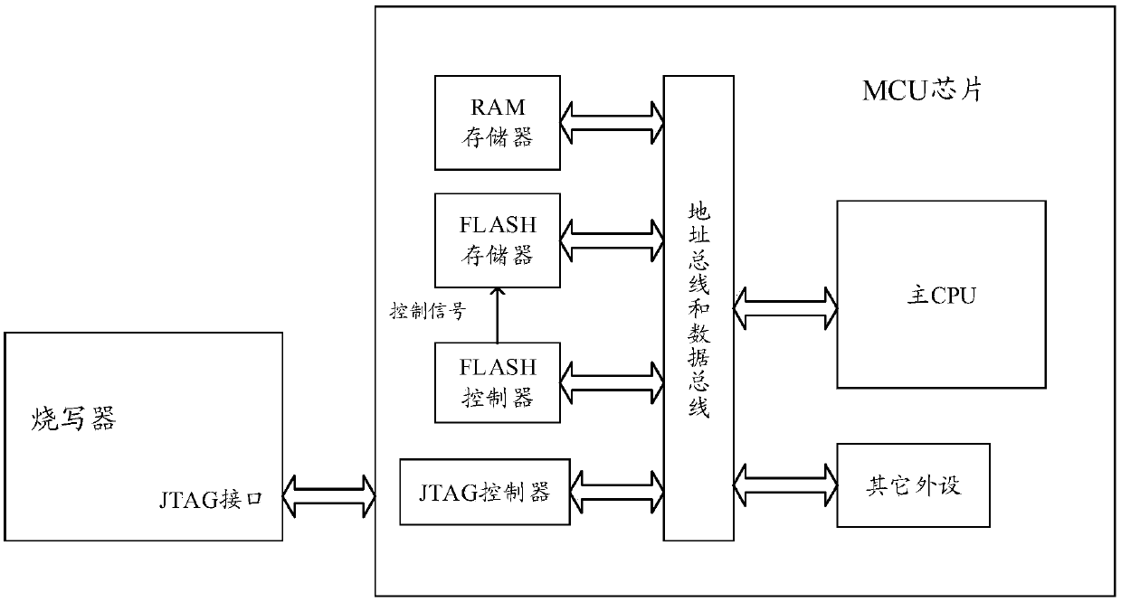
[0047] see figure 1 As shown, it is a schematic structural diagram of the Flash memory programming system of the present invention, the Flash memory programming system, wherein the system includes a programmer and a microcontroller, the programmer and the microcontroller The controller is connected through the JTAG interface, the microcontroller includes a RAM memory and a Flash memory, the RAM memory receives the self-programming program in the programmer, and the RAM memory segment receives the After the data to be programmed in the programmer, the current data section to be programmed is programmed into the Flash memory through the self-programming program until the programming of the data to be programmed is completed.

[0048] In a specific embodiment of the present invention, the microcontroller of th...


PUM


Abstract

The invention relates to a Flash memory programming system and method. The system comprises a programmer and a microcontroller. The programmer and the microcontroller are connected through a JTAG interface. The microcontroller comprises an RAM memory and a Flash memory. The RAM receives a self-programming program in the programmer, and after the RAM receives to-be-programmed data in the programmerin a segmented manner, a current to-be-programmed data segment is programmed into the Flash memory through the self-programming program until programming of the to-be-programmed data is completed. According to the flash memory programming system and the flash memory programming method, the communication time on the JTAG interface is shortened, the programming time of the flash memory is shortened, the programming efficiency is improved, and the flash memory programming system and the flash memory programming method have a wider application range.

Description

technical field [0001] The present invention relates to the field of embedded systems, in particular to the field of electronic technology, in particular to a flash memory programming system and method. Background technique [0002] Usually, the programming process of each byte in the microcontroller is to configure the address register and data register first, then start the programming of the control register, then read the programming status register, wait for the programming to complete, and finally read the Check out the data in the Flash memory to determine whether the programming is successful. Since every write of a byte requires the JTAG (JointTest Action Group Joint Test Action Group) controller to configure the relevant registers, and configuring each register requires entering the register configuration command, register address and register data, for 16-bit address line micro The controller needs to transmit at least 120 bits of data on the JTAG interface for e...

Claims


Application Information

Patent Timeline
Patent Type & Authority Applications(China)
IPC IPC(8): G06F8/654
Inventor 顾晓红孙红新赵海
Owner CRM ICBG (WUXI) CO LTD
Learn More