Pixel arrangement structure and related device

A pixel arrangement and pixel technology, applied in ion implantation plating, coating, instrument, etc., can solve the problem of large pixel distance

Pending Publication Date: 2019-08-16
BOE TECH GRP CO LTD
View PDF0 Cites 19 Cited by
  • Summary
  • Abstract
  • Description
  • Claims
  • Application Information

AI Technical Summary

Problems solved by technology

[0005] In view of this, an embodiment of the present invention provides a pixel arrangement structure, an organic electroluminescent display panel, a high-precision metal mask, and a display device to solve the problem of the large distance between pixels existing in existing OLED devices. The problem

Method used


Image

  • Pixel arrangement structure and related device
  • Pixel arrangement structure and related device
  • Pixel arrangement structure and related device

Examples


Embodiment Construction

[0036] In order to make the purpose, technical solution and advantages of the present invention clearer, the present invention will be further described in detail below in conjunction with the accompanying drawings. Apparently, the described embodiments are only some embodiments of the present invention, rather than all embodiments. Based on the embodiments of the present invention, all other embodiments obtained by persons of ordinary skill in the art without making creative efforts belong to the protection scope of the present invention.

[0037] The shapes and sizes of the components in the drawings do not reflect the real scale, but are only intended to schematically illustrate the content of the present invention.

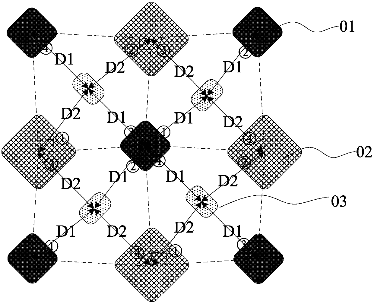
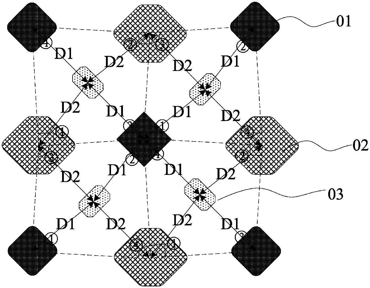
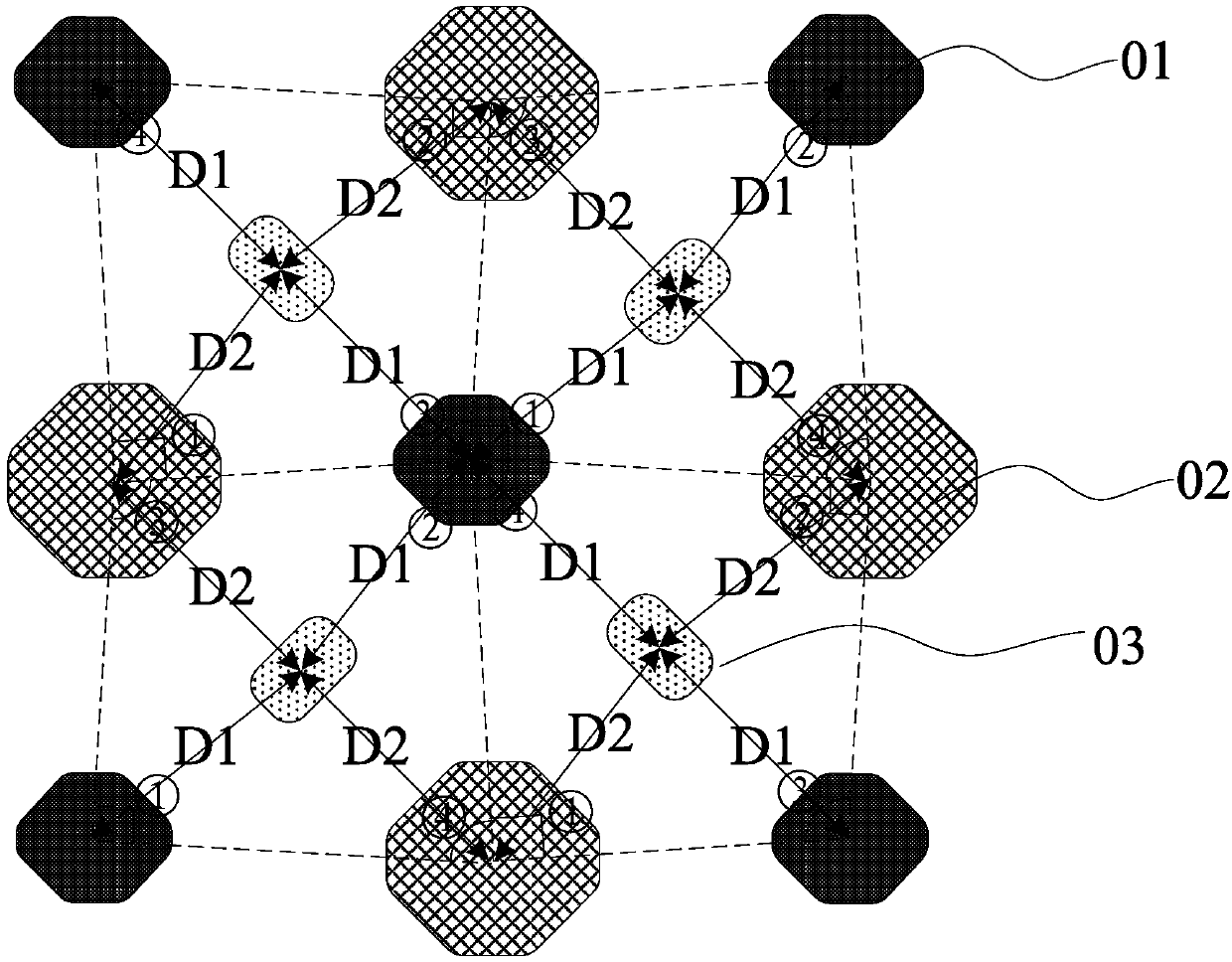
[0038] A pixel arrangement structure provided by an embodiment of the present invention, such as Figure 1 to Figure 3 As shown, it includes: the first sub-pixel 01, the second sub-pixel 02 and the third sub-pixel 03;

[0039] The first sub-pixel 01 is locate...


PUM


Abstract

The invention discloses a pixel arrangement structure and a related device. The first sub-pixels are located at the center position of first virtual quadrangles and four vertex angle positions of thefirst virtual quadrangles; second sub-pixels are located at the center position of the sides of the first virtual quadrangles; third sub-pixels are located in second virtual quadrangles, and the foursecond virtual quadrangles form one first virtual quadrangle. In the second virtual quadrangles, the center distances between the third sub-pixels and the two first sub-pixels are equal; and / or, the center distances between the third sub-pixels and the two second sub-pixels are equal. Compared to a pixel arrangement structure in the prior art, the first sub-pixels, the second sub-pixels and the third sub-pixels can be tightly arranged in the same process condition to reduce the distances between the adjacent pixels as much as possible, so that the pixel opening area is increased in the condition of the same resolution, the drive current of the display device is reduced, and the life of the display device is prolonged.

Description

technical field [0001] The invention relates to the field of display technology, in particular to a pixel arrangement structure, an organic electroluminescent display panel, a high-precision metal mask and a display device. Background technique [0002] Organic Light Emitting Diode (OLED) display devices are one of the hot spots in the field of flat panel display research today. Compared with liquid crystal displays, OLED display devices have low energy consumption, low production cost, self-illumination, wide viewing angle and response speed. At present, OLED display devices have begun to replace traditional Liquid Crystal Displays (LCDs) in the field of flat panel displays such as mobile phones, PDAs, and digital cameras. [0003] The structure of the OLED display device mainly includes: a base substrate, and pixels arranged in a matrix on the base substrate. Wherein, each pixel generally uses an organic material to form an organic electroluminescent structure at a corres...

Claims


Application Information

Patent Timeline
Patent Type & Authority Applications(China)
IPC IPC(8): H01L27/32C23C14/24C23C14/12C23C14/04
CPCC23C14/042C23C14/12C23C14/24H10K59/353G09G2300/0452G09G3/3208H10K59/352G09G3/3225H10K59/121H10K59/122
Inventor 肖志慧刘月张浩瀚白珊珊
Owner BOE TECH GRP CO LTD
Why Eureka
Try Eureka