

Method for measuring secondary electron emission coefficient of dielectric material
A technology of secondary electron emission and dielectric materials, applied in the field of physical electronics
- Summary
- Abstract
- Description
- Claims
- Application Information
AI Technical Summary
Problems solved by technology
Method used
Image

Examples
Embodiment Construction
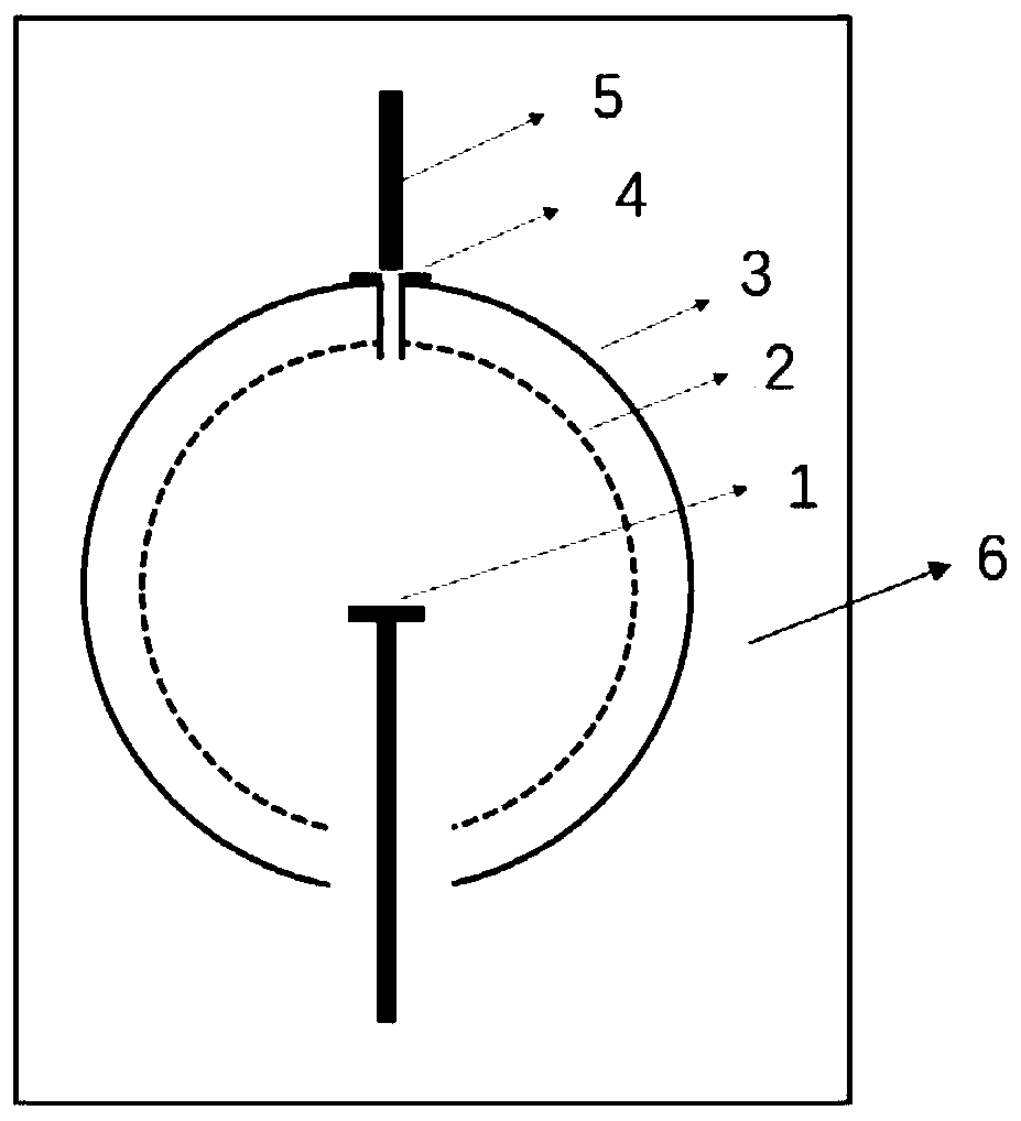
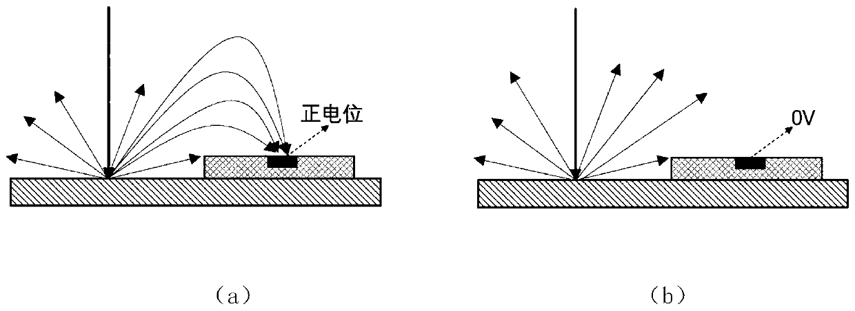
[0030] The invention provides a new method for neutralizing the surface charge of a dielectric material and a corresponding method for testing the secondary electron emission coefficient. This method weakens the measurement error introduced by the charge accumulation effect, and then can measure the secondary electron emission coefficient of the dielectric material under different incident energies in an accurate and effective way. And this method can measure all the secondary electron emission coefficients of the sample material under different incident energies in one complete measurement. During the whole test process, there is no need to move the sample, replace the electronic structure and other operations. The operation is simple and convenient, and the test result is accurate. The neutralization method has a simple structure, a wide range of applications, and effectively prevents the accumulation of negative charges caused by excessive neutralization on the basis of full...
PUM
 Abstract
Description
Claims
Application Information