Giant dielectric thin film transistor

A technology of thin-film transistors and giant dielectrics, applied in transistors, circuits, electrical components, etc., can solve problems such as limited application range, slow ion speed, and poor temperature stability of devices

Inactive Publication Date: 2019-08-20
SOUTH CHINA UNIV OF TECH
View PDF3 Cites 1 Cited by
  • Summary
  • Abstract
  • Description
  • Claims
  • Application Information

AI Technical Summary

Problems solved by technology

Ferroelectric ceramic materials have a relative permittivity greater than 100, but since the ferroelectric material undergoes a ferroelectric-paraelectric phase transition at the Curie temperature, the dielectric constant of the ferroelectric material changes significantly with temperature, resulting in a temperature increase of the device. The stability becomes poor, which limits its application

Method used


Image

  • Giant dielectric thin film transistor
  • Giant dielectric thin film transistor
  • Giant dielectric thin film transistor

Examples


Embodiment 1

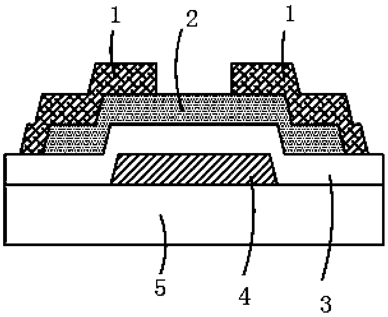
[0042] A giant dielectric thin film transistor is provided with a gate 4, a semiconductor 2 and a gate insulating layer 3 between the gate 4 and the semiconductor 2.

[0043] The gate insulating layer 3 is made of a giant dielectric material as the gate insulating layer 3 .

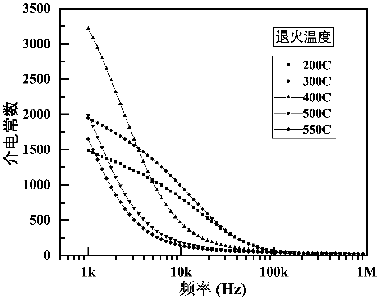
[0044] When the giant dielectric material is in the state of a ceramic block, the relative permittivity is greater than 10,000 at a frequency of 1 kHz, and when the giant dielectric material is in a thin film state, the relative permittivity is greater than 500 at 1 kHz.

[0045] Giant dielectric materials are non-ferroelectric ceramic materials.

[0046] The giant dielectric material of the present invention is CaCu 3 Ti 4 o 12 or CaCu 3 Ti 4 o 12 modified materials. The specific giant dielectric material of the present embodiment is CaCu 3 Ti 4 o 12 .

[0047] The gate insulating layer 3 is a giant dielectric material thin film prepared from a giant dielectric material at a temperature lower ...

Embodiment 2

[0056] A kind of giant dielectric thin film transistor, other characteristics are identical with embodiment 1, difference is: giant dielectric material of the present invention is A(Fe 1 / 2 G 1 / 2 )O 3 , wherein A is Ba, Sr, Ca or Pb, and G is Nb, Ta or Sb. The specific A(Fe 1 / 2 G 1 / 2 )O 3 , where A is Ba, G is Nb, that is, Ba(Fe 1 / 2 Nb 1 / 2 )O 3 .

[0057] The semiconductor 2 of the present invention is an oxide semiconductor 2, and the oxide semiconductor 2 contains Zn.

[0058] It should be noted that A in the present invention may be Ba, or Sr, Ca or Pb, and the specific implementation method depends on the actual situation. In the present invention, G can be Nb, Ta or Sb, and the specific implementation method depends on the actual situation.

[0059] It should be noted that the oxide semiconductor of the present invention may contain Zn, one of Sn, In, Cd or Ga, or a combination of various elements, and the specific implementation method depends on the actual situ...

Embodiment 3

[0062] A kind of giant dielectric thin film transistor, other characteristics are identical with embodiment 1, difference is: the giant dielectric material of the present invention is (M, N)-doped NiO, and wherein M is Li, Na or K, and N is Ti, Al, Si or Ta. Specifically, in this embodiment, M is Li and N is Ti, that is, (Li, Ti)-doped NiO.

[0063] It should be noted that M in the present invention can be Li, Na or K, and the specific implementation method depends on the actual situation. In the present invention, N can be Ti, or Al, Si or Ta, and the specific implementation method depends on the actual situation.

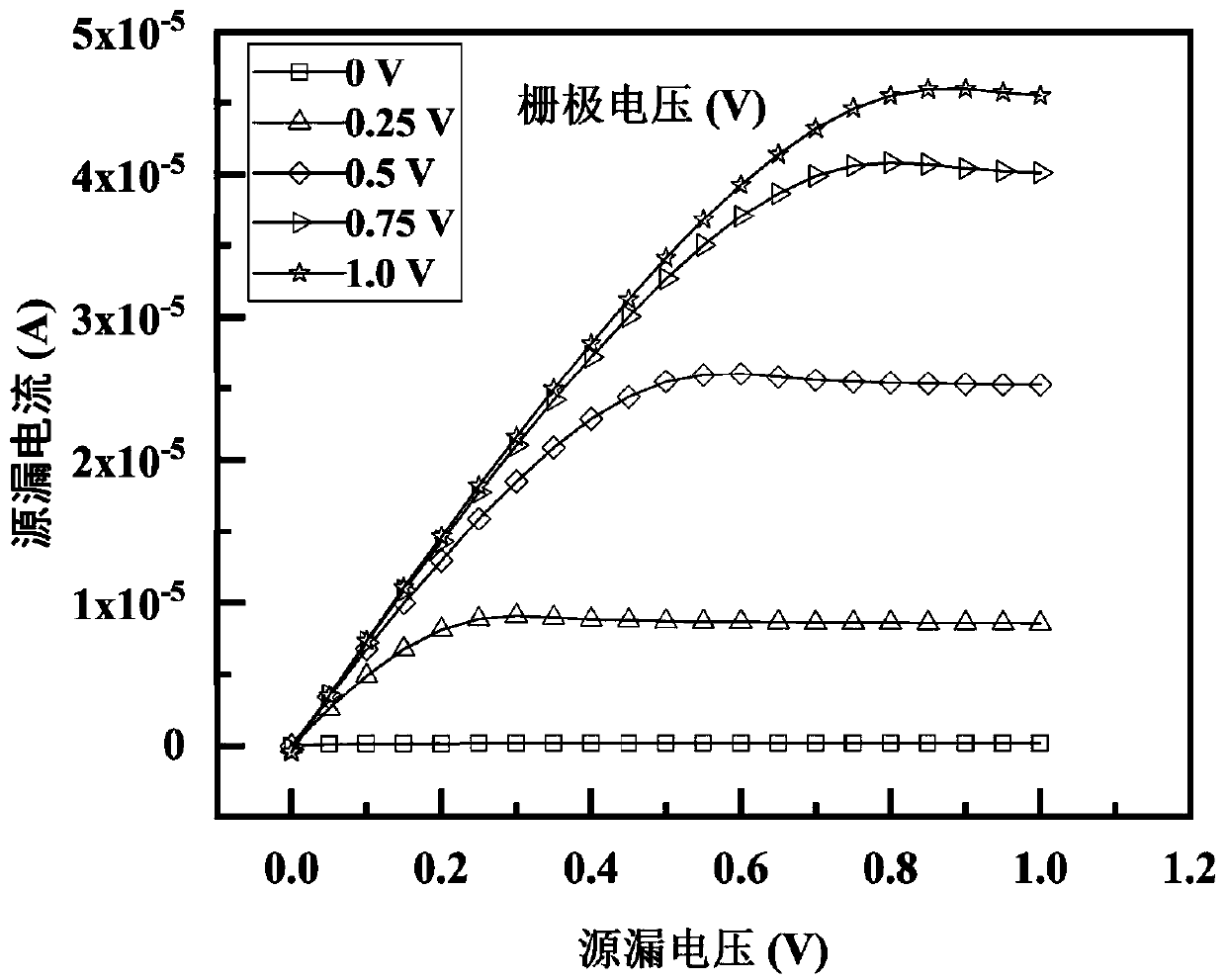
[0064] Compared with the gate insulating layer 3 of the TFT with the ion electric double layer, the giant dielectric thin film transistor of the present invention has the advantage of good frequency response, the frequency response of the inverter is greater than 500Hz, and low power consumption circuit, so it has great advantages in the display field Good appli...


PUM


Abstract

The invention relates to a giant dielectric thin film transistor, which is provided with a grid electrode, a semiconductor and a gate insulating layer located between the grid electrode and the semiconductor layer, wherein the gate insulating layer adopts a giant dielectric material; the relative dielectric constant is greater than 10000 at the frequency of 1kHz when the giant dielectric materialis in a ceramic block state, and the relative dielectric constant is greater than 500 at the frequency of 1kHz when the giant dielectric material is in a thin film state; and the giant dielectric material is a non-ferroelectric ceramic material. Compared with a TFT adopting ionic double electric layer to serve as the gate insulating layer, the giant dielectric thin film transistor of the inventionhas the advantage of good frequency response, the frequency response of an inverter is greater than 500Hz, and the circuit is low in consumption, thereby having good application potential in the field of displays. Meanwhile, the giant dielectric thin film transistor of the invention is prepared by adopting the non-ferroelectric material, so that there is no hysteresis phenomenon.

Description

technical field [0001] The invention relates to the technical field of thin film transistors, in particular to a giant dielectric thin film transistor. Background technique [0002] The dielectric material used for the gate insulating layer of thin film transistors is usually SiO 2 (relative dielectric constant is about 3.9), SiNx (relative dielectric constant is about 7), etc., the dielectric constant is low, resulting in higher operating voltage and higher power consumption. In order to reduce the operating voltage and reduce power consumption, high-k dielectric materials (such as ZrO 2 、Al 2 o 3 , HfO 2 etc.) is a common practice, but the relative permittivity of these materials is usually lower than 50, and there is still a lot of room for improvement. Ferroelectric ceramic materials have a relative permittivity greater than 100, but since the ferroelectric material undergoes a ferroelectric-paraelectric phase transition at the Curie temperature, the dielectric cons...

Claims


Application Information

Patent Timeline
IPC IPC(8): H01L29/786H01L29/51
CPCH01L29/517H01L29/786
Inventor 兰林锋陈卓彭俊彪
Owner SOUTH CHINA UNIV OF TECH
Why Eureka
Try Eureka