Wafer cleaning apparatus and wafer cleaning method

A technology for cleaning devices and wafers, applied in electrical components, semiconductor/solid-state device manufacturing, circuits, etc., can solve the problems of difficult to remove wafer contamination, decreased effect of surfactants, and deterioration of wafer surface quality. The effect of standby time, shortening cycle, and reducing metal contamination parts

Inactive Publication Date: 2019-08-30
XIAN ESWIN MATERIAL TECH CO LTD +1
View PDF10 Cites 2 Cited by
  • Summary
  • Abstract
  • Description
  • Claims
  • Application Information

AI Technical Summary

Problems solved by technology

[0005] In this case, the effect of the surfactant decreases with the passage of time, and the direct mechanical friction between the brush mainly composed of nylon and the surface of the wafer will cause scratches on the surface of the wafer, etc. The quality of the round surface deteriorates; on the other hand, there is also the problem of managing the life time (Life time) of the brush during use; in addition, the abrasive dust removed by the upper bru

Method used


Image

  • Wafer cleaning apparatus and wafer cleaning method

Examples


Embodiment Construction

[0025] The following will clearly and completely describe the technical solutions in the embodiments of the present invention with reference to the accompanying drawings in the embodiments of the present invention. Obviously, the described embodiments are some of the embodiments of the present invention, but not all of them. Based on the embodiments of the present invention, all other embodiments obtained by persons of ordinary skill in the art without creative efforts fall within the protection scope of the present invention.

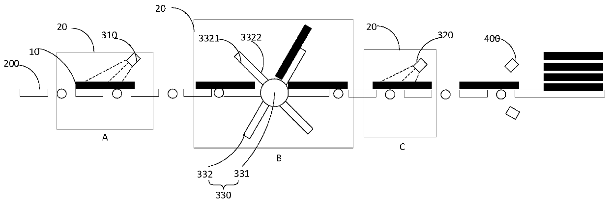
[0026] Aiming at the problems in the prior art that the mechanical cleaning method of wafers has poor cleaning effect and is prone to scratches, which affects product quality, the embodiment of the present invention provides a wafer cleaning device and a wafer cleaning method, which can improve cleaning efficiency. Effect, without mechanical friction cleaning, improve cleaning strength and product quality.

[0027] like figure 1 As shown, the wafer cl...


PUM


Abstract

The invention provides a wafer cleaning apparatus and a wafer cleaning method. The apparatus comprises a conveyor belt, wherein a first cleaning zone, an overturning zone and a second cleaning zone are successively disposed in the conveying direction of the conveyor belt; in the first cleaning zone, a first nozzle for spraying a cleaning liquid onto the first surface of a wafer on the conveyor belt is disposed above the conveyor belt; in the second cleaning zone, a second nozzle for spraying a cleanser onto the second surface, opposite to the first surface, of the wafer is disposed above the conveyor belt; and in the overturning zone, an overturning mechanism for overturning the wafer is disposed. The wafer cleaning apparatus sprays the cleaning liquid onto the surfaces of the wafer by the nozzles instead of a traditional mechanical cleaning method, reduces the scratches on the surfaces of the wafer, improves the surface quality of a product, changes a traditional batch cleaning modeto a single wafer cleaning mode, shortens the standby time of the cleaning project, shortens the cycle, improves productivity, and improves cleaning force, quality and productivity by double-sided cleaning.

Description

technical field [0001] The invention relates to the field of semiconductor material manufacturing, in particular to a wafer cleaning device and a wafer cleaning method. Background technique [0002] As a material for manufacturing semiconductor elements, silicon wafers (Si wafers) are widely used. A silicon wafer is a wafer in which the same type of silicon is grown on the silicon surface. Silicon wafers are widely used because they are excellent in the purity and crystallization properties of regions where semiconductors are integrated, and are beneficial to the yield and device characteristics of semiconductor devices. [0003] Usually, the surface of the lapped wafer is polluted by lapping oil and powder sludge. When the next project is carried out in this state, in addition to the scratches on the surface of the wafer, the metal components in the lapping powder (Lapping powder) may contaminate the equipment of the next project. Pollutants on the round surface should b...

Claims


Application Information

Patent Timeline
IPC IPC(8): H01L21/67H01L21/02
CPCH01L21/02041H01L21/02057H01L21/02082H01L21/67017H01L21/67023
Inventor 姜镕
Owner XIAN ESWIN MATERIAL TECH CO LTD
Why Eureka
Try Eureka