Testing structure and method for back drill alignment degree of 5G circuit board

A technology of test structure and test method, which is applied in the field of PCB board manufacturing, can solve problems such as difficulties, missed inspection of boards, and long time consumption, and achieve the effect of large amount of detection, fast speed, and improved detection efficiency

Inactive Publication Date: 2019-08-30
AOSHIKANG TECH CO LTD
View PDF4 Cites 4 Cited by
  • Summary
  • Abstract
  • Description
  • Claims
  • Application Information

AI Technical Summary

Problems solved by technology

During the back drilling process, if the back drill and the first drill have offset holes, it is very easy to cause the copper in the first drill part of the hole wall to be completely drilled, resulting in signal transmission distortion
[0003] At present, slices are usually used to check the alignment of the back drill, and the inspection workload is heavy, time-consuming, laborious, and difficult to judge.
This method of slice inspection is inefficient and time-consuming, and it is easy to miss inspections of boards with poor back-drilling accuracy, resulting in batch scrapping and even abnormal boards flowed to customers, resulting in immeasurable losses

Method used


Image

  • Testing structure and method for back drill alignment degree of 5G circuit board
  • Testing structure and method for back drill alignment degree of 5G circuit board
  • Testing structure and method for back drill alignment degree of 5G circuit board

Examples


Embodiment Construction

[0028] In order to make the object, technical solution and advantages of the present invention clearer, the present invention will be further described in detail below in conjunction with the accompanying drawings and embodiments. It should be understood that the specific embodiments described here are only used to explain the present invention, not to limit the present invention.

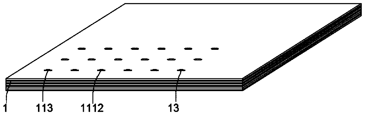
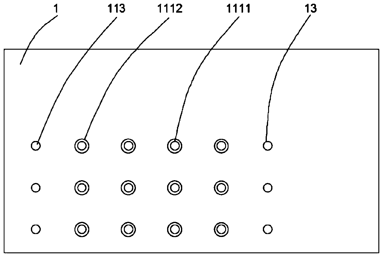
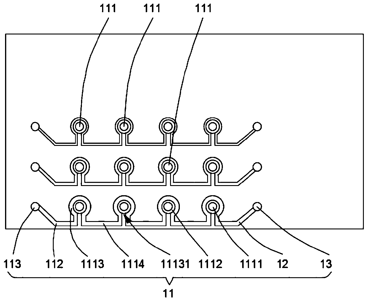
[0029] In the present embodiment, the number of layers n of the core board 1 of the PCB board is 10, the quantity w of the test unit 11 is 3, and the quantity j of the small group 111 of each test unit 11 in the 3 test units 11 is all 4, need The number of layers m of the back drilled core board 1 is 4, that is, the back drill 1112 on the first to fourth layers of the core board 1 on the PCB needs to be drilled off, the width d1 of the ring line 1113 on the first layer is 4mil, and a is 1mil , the back-drilling alignment is set to 4mil, what needs to be explained here is the width of the ring line ...


PUM


Abstract

The utility model discloses a testing structure for the back drill alignment degree of a 5G circuit board. The testing structure comprises first to nth layers of core plates which are sequentially laminated from top to bottom, wherein n is a natural number, and n is greater than 2. The first to nth layers of core plates further comprise: first to wth testing units, outgoing lines and second testing columns. The first to wth testing units and the outgoing lines are all arranged on the mth core plate, the second testing columns penetrate through the mth core plate, the rth testing unit is connected with the (r + 1) th testing unit through the outgoing lines and the second testing columns are connected with the outgoing lines, wherein r, w and m are all natural numbers, and 0<r<w-1, and 1<m<n. According to the invention, a circuit is designed on the core board on a PCB, and the back drilling offset is detected by testing whether the current passes through a loop line, so, in this way, theback drilling offset of the PCB can be detected on a large scale, the speed is high, the detection amount is large, and the detection efficiency is improved. Meanwhile, an accurate offset range valuecan be provided, and a basis is provided for later adjustment.

Description

technical field [0001] The invention belongs to the technical field of PCB board manufacturing, and in particular relates to a test structure and method for back-drilling alignment of a 5G circuit board. Background technique [0002] In the production of PCB, the function of back drilling is to drill out the through-hole section that does not play any connection or transmission role, so as to avoid reflection, scattering, delay, etc. of high-speed signal transmission, which will bring "distortion" to the signal. During the back-drilling process, if the back-drill and the first-drill have offset holes, it is very easy to cause the copper in the first-drill part of the hole wall to be completely drilled, resulting in signal transmission distortion. [0003] At present, slices are usually used to check the alignment of the back drill, and the inspection workload is heavy, time-consuming and labor-intensive, and it is difficult to judge. This slice inspection method is ineffici...

Claims


Application Information

Patent Timeline
Patent Type & Authority Applications(China)
IPC IPC(8): H05K1/02G01B7/00
CPCG01B7/00G01B7/003H05K1/0268H05K2203/162
Inventor 曾海强
Owner AOSHIKANG TECH CO LTD
Why Eureka
Try Eureka