Electronic device and method for kickback noise reduction of switched capacitive loads and method of operating the electronic device

a switched capacitive load and electronic device technology, applied in the field of electronic device and method for reducing the kickback noise of switched capacitive loads and the field of operating the electronic device, can solve the problems of low performance, simple buffer having a rather large offset, etc., and achieve the effect of small input capacitance, low noise reduction, and high offs

Active Publication Date: 2014-12-30
TEXAS INSTR INC
View PDF7 Cites 1 Cited by
  • Summary
  • Abstract
  • Description
  • Claims
  • Application Information

AI Technical Summary

Benefits of technology

[0010]According to an aspect of the invention, there is an electronic device comprising a first stage having an input capacitance, a switch, a buffer and a second stage. The second stage has an input that is sensitive to charge injection and / or a voltage glitch. An input of the buffer and the input of the second stage may be coupled together at a first node. The first node may then be configured to be coupled to a voltage source for supplying a reference voltage to the input of the first stage having the input capacitance. In a first configuration of the switch, the switch may be arranged to connect the input of the first stage to the first node. Also in the first configuration, the switch disconnects the input of the first stage from an output of the buffer. In a second configuration of the switch, the switch is arranged to connect the input of the first stage to the output of the buffer and to disconnect the input of the first stage from the first node. This aspect of the invention provides that the input of the first stage is either driven by the buffer or connected to the first node. The input capacitance of the first stage can then be charged by the buffer. The buffer itself can have a smaller input capacitance than the first stage. Furthermore, the buffer can be switched off after having charged the input capacitance of the first stage and when the switch is in the first configuration. This saves power. The buffer may be very simple having a rather large offset (input related offset) and low performance. In the context of this invention, the buffer is considered to be an amplifier with a gain of one. The output signal of the buffer may then deviate from the input voltage (reference voltage level at the first node) by the offset. This invention provides that a buffer with a rather high offset can be used and that kickback noise at the input of the second stage is still reduced. Furthermore, also the power consumption can be reduced, as the buffer can have low power consumption and be switched off after charging the input of the first stage.
[0011]In another aspect of the invention, the electronic device may further be configured such that the default configuration of the switch is the second configuration. This provides that the input of the first stage is not accidentally connected to the first node.
[0012]In another aspect of the invention, the electronic device may further be configured to activate the buffer before the switch switches from the second to the first configuration. This provides that the input capacitance is charged before the input of the first stage is connected to the first node, i.e. before it is connected to the reference voltage source. This helps to reduce the amount of kickback noise.
[0015]In still another aspect of the invention, the electronic device may further be configured to switch the switch from the first into the second configuration before changing the voltage and / or the charge of the input capacitance at the input of the first stage. Activating and deactivating the first stage generally relates to a change of the voltage and / or charge of the input capacitance of the first stage. The first stage can be an active device that is switched on or off. However, in an embodiment, it may also be a switched capacitor or a capacitor that is configured to increase or decrease the charge and / or the voltage. These changes of the charge and / or voltage of the input capacitor should only occur while the switch is in the second configuration. The buffer can block the kickback noise even if it is switched off.
[0019]The invention also provides a method of operating the electronic device configured in accordance with the aspects and embodiments of the invention, accordingly, the buffer may be activated. The first stage may then be activated. However, the first stage may also be activated before the buffer, or they may be activated at the same time. The switch is in the default position, i.e. in the second configuration. The switch is then switched from the second configuration to the first configuration. The switch is advantageously only switched after the buffer output has settled. According to aspects of the invention, the buffer may have an offset. This means that the output of the buffer settles to an output voltage level that deviates from the reference voltage level provided by the reference voltage source by the offset voltage. An aspect of this invention provides that a buffer with rather high offset but rather small input capacitance can be used and the kickback noise at the input of the second stage is still reduced.

Problems solved by technology

The buffer may be very simple having a rather large offset (input related offset) and low performance.

Method used


Image

  • Electronic device and method for kickback noise reduction of switched capacitive loads and method of operating the electronic device
  • Electronic device and method for kickback noise reduction of switched capacitive loads and method of operating the electronic device
  • Electronic device and method for kickback noise reduction of switched capacitive loads and method of operating the electronic device

Examples


Embodiment Construction

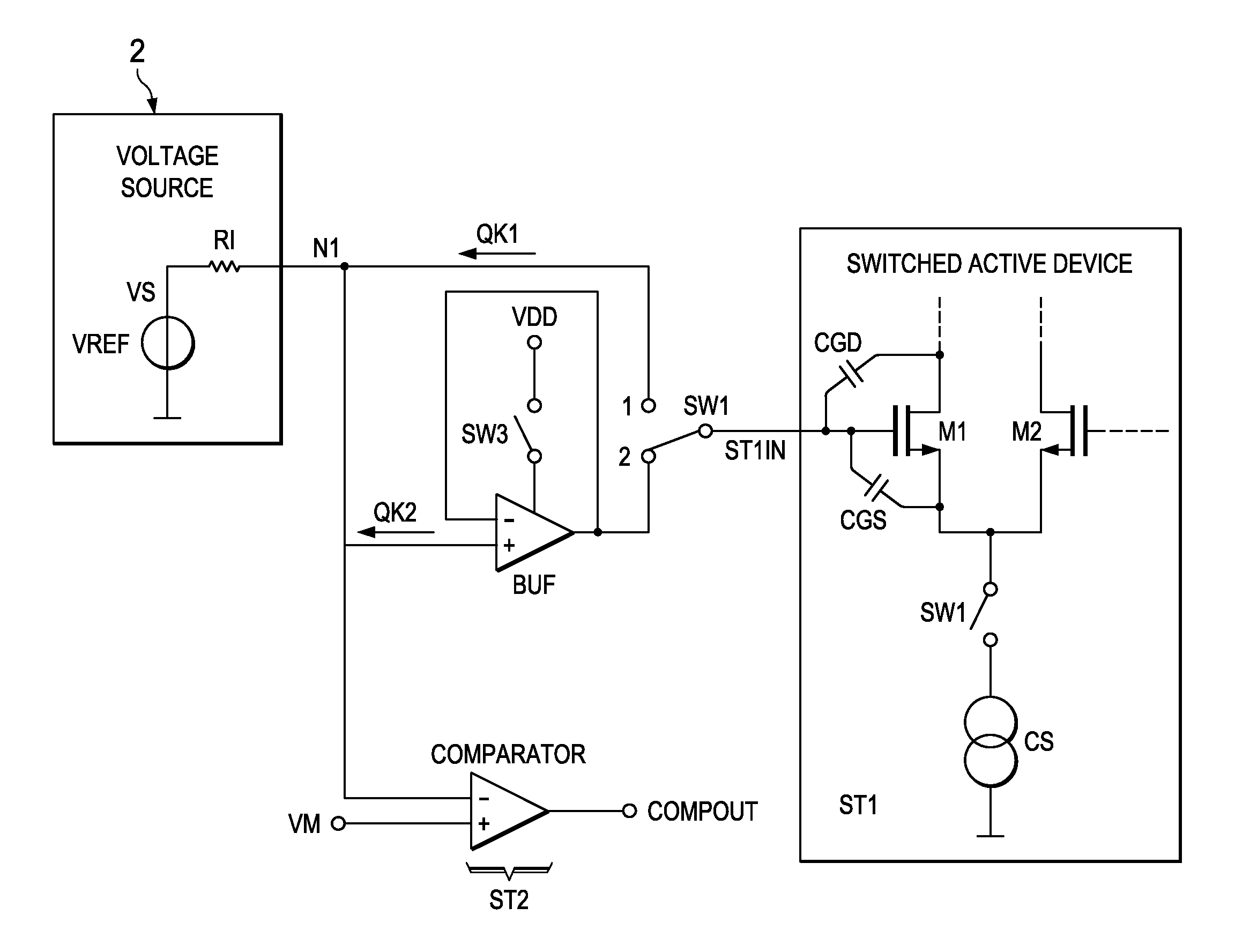
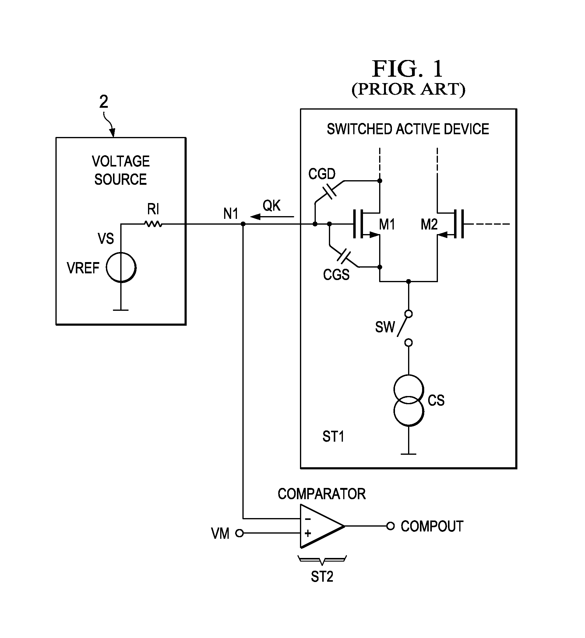
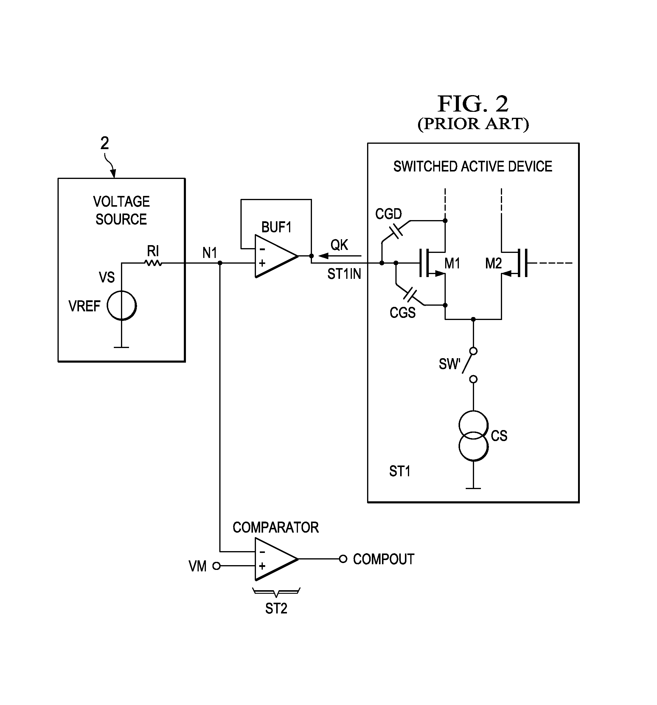
[0026]FIG. 3 shows a simplified diagram of an embodiment of the invention. There is an electronic device 1 comprising a first stage ST1 having an input ST1IN. The input has in input capacitance C1 which is represented by capacitor C1 which can be coupled with the other side to any kind of reference of supply voltage VX. There is a second stage ST2 having an input ST2IN which is sensitive to charge injection and / or glitches. The second stage ST2 may be a comparator or an amplifier or the like. There is a buffer BUF. The buffer BUF may be a non-inverting amplifier with gain one. The positive input of the buffer (operational amplifier) is connected to the first node N1. The output of the buffer (BUF) is (BUFOUT). There is a reference voltage source VS, which is configured to supply a reference voltage VREF to the first node N1. The reference voltage VREF is conceived to be fed to the input ST1IN of the first stage ST1. The voltage source VS has an output resistance or impedance RI. The...


PUM


Abstract

An electronic device which includes a first stage having an input capacitance, a switch, a buffer and a second stage having an input sensitive to charge injection and / or voltage glitches. An input of the buffer and the input of the second stage are coupled together at a first node which is configured to be coupled to a voltage source for supplying a reference voltage to the input of the first stage having the input capacitance. In a first configuration of the switch, the switch is arranged to either connect the input of the first stage to the first node and to disconnect the input of the first stage from an output of the buffer. In a second configuration of the switch, to connect the input of the first stage to the output of the buffer and to disconnect the input of the first stage from the first node.

Description

CROSS-REFERENCE TO RELATED APPLICATIONS[0001]This patent application claims priority from German Patent Application No. 10 2010 048 440.7, filed Oct. 15, 2010, which is incorporated herein by reference in its entirety.FIELD OF THE INVENTION[0002]The invention relates to an electronic device and a method for kickback noise reduction when switching capacitive loads and a method of manufacturing such an electronic device.BACKGROUND OF THE INVENTION[0003]Integrated electronic semiconductor devices often have to cope with capacitive loads that have to be charged and discharged to certain voltage levels. There are stages with an input capacitance, as for example comparators, buffers or amplifiers that are switched on and off, as well as simple capacitances or cables.[0004]If the drain current of a MOS transistor changes its gate-source voltage must change, too and therefore the gate charge must change. If an amplifier with a MOS input transistor is switched on or off (i.e. the bias curren...

Claims


Application Information

Patent Timeline
Patent Type & Authority Patents(United States)
IPC IPC(8): H03K17/687H03F3/72
CPCH01L2924/0002H03F3/72H03F2203/45136H03M1/0845H01L2924/00
Inventor PESCHKE, CARLOMUELLNER, ERNST
Owner TEXAS INSTR INC
Why Eureka
Try Eureka