
Structures and techniques for using semiconductor body to construct SCR, DIAC, or triac
a technology of semiconductor body and structure, applied in the direction of semiconductor devices, electrical equipment, transistors, etc., can solve the problems of destroying mos gate oxides, damaging metallurgical junctions, damaging delicate integrated circuits, etc., and achieves low input capacitance, high esd immunity, and small i/o size
- Summary
- Abstract
- Description
- Claims
- Application Information
AI Technical Summary
Benefits of technology
Problems solved by technology
Method used
Image

Examples
Embodiment Construction
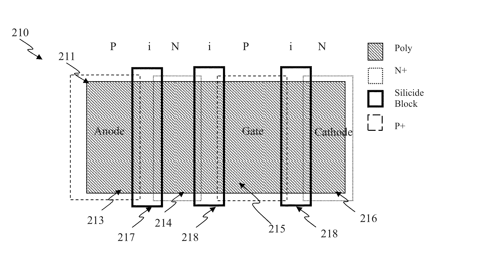
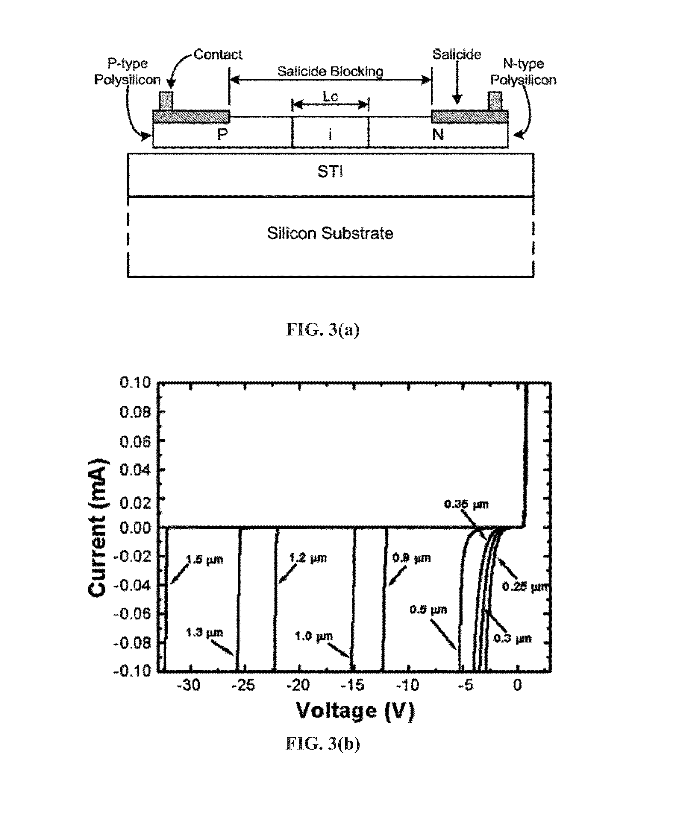
[0049]Embodiments disclosed herein use an ESD structure with ring-shape diodes. The diodes can comprise P+ and N+ implants on a polysilicon or active region body on an insulated substrate with the P+ and N+ implants separated by a gap. The gap can be covered by a silicide block layer (SBL) and overlapping into both P+ and N+ areas. The diode can also be N+ active region on a P type substrate or P+ active region on an N well. The isolation between the P+ and N+ active regions can, for example, be LOCOS (LOCal Oxidation), STI (Shallow Trench Isolation), dummy gate, or SBL in standard CMOS processes. Since the P+ and N+ implants, active regions, and polysilicon are readily available in standard CMOS logic processes, these devices can be formed in an efficient and cost effective manner. There are no additional masks or process steps to save costs. The ESD protection device can also be included within an electronic system.
[0050]FIG. 4 shows a block diagram of an ESD protection device 30 ...
PUM
 Abstract
Description
Claims
Application Information