Structures and techniques for electro-static discharge (ESD) protection using ring structured diodes

a diode and structure technology, applied in the direction of diodes, semiconductor devices, electrical equipment, etc., can solve the problems of destroying mos gate oxides, damaging metallurgical junctions, damaging delicate integrated circuits, etc., and achieves low input capacitance, high esd immunity, and small i/o size

Inactive Publication Date: 2014-05-15
ATTOPSEMI TECH CO LTD
View PDF3 Cites 74 Cited by
  • Summary
  • Abstract
  • Description
  • Claims
  • Application Information

AI Technical Summary

Benefits of technology

[0012]Embodiments of ESD protection using ring structures of diodes are disclosed. The diodes constructed from polysilicon or active region body on insulated

Problems solved by technology

When an integrated circuit is touched by a human bodies during handling, a very high voltage (˜5 KV) and a high current (˜2 A) may be generated that can damage a delicate integrated circuit.
The high voltage generated may breakdown MOS gate oxides, and the high power generated by high current may damage the metallurgical junctions.
Firstly, as gate oxide of the MOS devices becomes thinner, it becom

Method used


Image

  • Structures and techniques for electro-static discharge (ESD) protection using ring structured diodes
  • Structures and techniques for electro-static discharge (ESD) protection using ring structured diodes
  • Structures and techniques for electro-static discharge (ESD) protection using ring structured diodes

Examples


Embodiment Construction

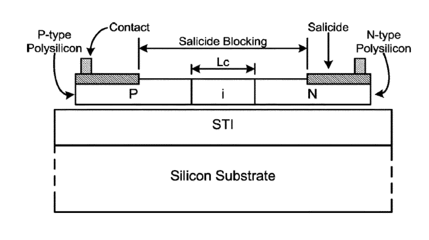
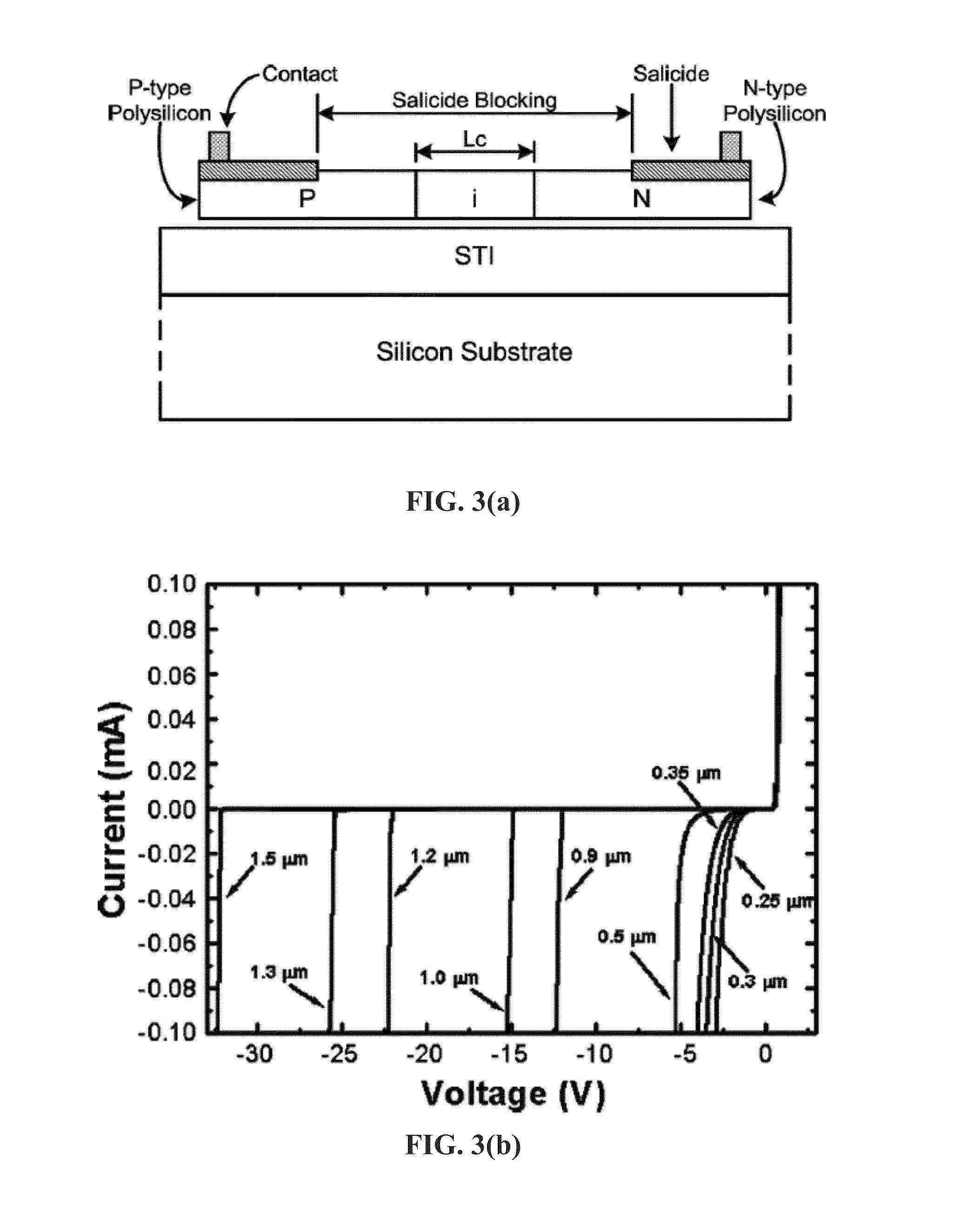
[0049]Embodiments disclosed herein use an ESD structure with ring-shape diodes. The diodes can comprise P+ and N+ implants on a polysilicon or active region body on an insulated substrate with the P+ and N+ implants separated by a gap. The gap can be covered by a silicide block layer (SBL) and overlapping into both P+ and N+ areas. The diode can also be N+ active region on a P type substrate or P+ active region on an N well. The isolation between the P+ and N+ active regions can, for example, be LOCOS (LOCal Oxidation), STI (Shallow Trench Isolation), dummy gate, or SBL in standard CMOS processes. Since the P+ and N+ implants, active regions, and polysilicon are readily available in standard CMOS logic processes, these devices can be formed in an efficient and cost effective manner. There are no additional masks or process steps to save costs. The ESD protection device can also be included within an electronic system.

[0050]FIG. 4 shows a block diagram of an ESD protection device 30 ...


PUM


Abstract

Electro-Static Discharge (ESD) protection using at least one ring-shape diode is disclosed. The ring-shape diode can be constructed from polysilicon, active region body on insulated substrate, or junction diode on silicon substrate. The diodes can have a first type of implant in an outer ring and a second type of implant in an inner ring to serve as two terminals of a diode coupled through contacts, vias, or metals. The two types of implant ring regions are separated with an isolation structure. The isolation can be LOCOS, STI, dummy gate, or silicide block layer (SBL). The ESD structure has at least a ring-shape diode with a first terminal coupled to an I/O pad and the second terminal coupled to a first supply voltage. The contours of the ring-shape diode can be circles, polygons, or other shapes. The ring-shape ESD structures can be multiple and be constructed in concentric manner.

Description

CROSS-REFERENCE TO RELATED APPLICATIONS[0001]This application claims priority benefit of U.S. Provisional Patent Application No. 61 / 560,159, filed on Nov. 15, 2011 and entitled “Using Ring-Shape Polysilicon Diodes for Electro-Static Discharge (ESD) Protection,” which is hereby incorporated herein by referenceBACKGROUND OF THE INVENTION[0002]1. Field of the Invention[0003]The present invention relates to Electro-Static Discharge (ESD) protection, i.e. using mechanism, device, circuit, apparatus, or any means to protection an integrated circuit from ESD damages.[0004]2. Description of the Related Art[0005]Human bodies may carry a lot of electrostatic charges. When an integrated circuit is touched by a human bodies during handling, a very high voltage (˜5 KV) and a high current (˜2 A) may be generated that can damage a delicate integrated circuit. The high voltage generated may breakdown MOS gate oxides, and the high power generated by high current may damage the metallurgical junction...

Claims


Application Information

Patent Timeline
IPC IPC(8): H01L29/861H01L29/04H01L29/66
CPCH01L29/861H01L29/6609H01L29/04H01L29/402H01L29/456H01L29/458H01L29/66113H01L29/66121H01L29/66128H01L29/66136H01L29/8611H01L29/868H01L29/87H01L29/0692H01L27/0262
Inventor CHUNG, SHINE C.
Owner ATTOPSEMI TECH CO LTD
Why Eureka
Try Eureka