Structures and techniques for using mesh-structure diodes for electro-static discharge (ESD) protection

a technology of electro-static discharge and diodes, applied in the direction of emergency protective circuit arrangements, basic electric elements, etc., can solve the problems of destroying mos gate oxides, damaging metallurgical junctions, and damaging delicate integrated circuits, etc., to achieve low input capacitance, high esd immunity, and small i/o size

Inactive Publication Date: 2014-05-15
ATTOPSEMI TECH CO LTD
View PDF0 Cites 61 Cited by
  • Summary
  • Abstract
  • Description
  • Claims
  • Application Information

AI Technical Summary

Benefits of technology

[0012]Embodiments of ESD protection using mesh structures of diodes are disclosed. The diodes constructed from polysilicon or active region body can be fabricated from standard bulk or SOI CMOS logic processes to achieve high ESD immunity, low input capacitance, small I / O size and low cost.

Problems solved by technology

When an integrated circuit is touched by a human bodies during handling, a very high voltage (˜5KV) and a high current (˜2 A) may be generated that can damage a delicate integrated circuit.
The high voltage generated may breakdown MOS gate oxides, and the high power generated by high current may damage the metallurgical junctions.
Firstly, as gate oxide of the MOS devices becomes thinner, it becomes more vulnerable to ESD damages due to aggressive scaling.
Thirdly, high speed and high frequency circuits in an integrated circuit require very small input capacitance and yet good ESD protection.
However, good ESD protection often requires large silicon area and high input capacitance.
The area of the diodes tends to be very large for better ESD immunity, but the large area is relatively costly.

Method used


Image

  • Structures and techniques for using mesh-structure diodes for electro-static discharge (ESD) protection
  • Structures and techniques for using mesh-structure diodes for electro-static discharge (ESD) protection
  • Structures and techniques for using mesh-structure diodes for electro-static discharge (ESD) protection

Examples


Embodiment Construction

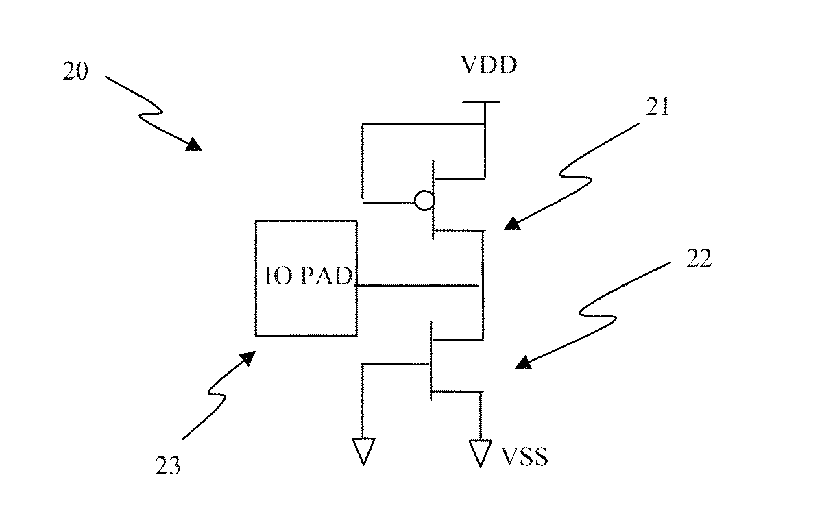
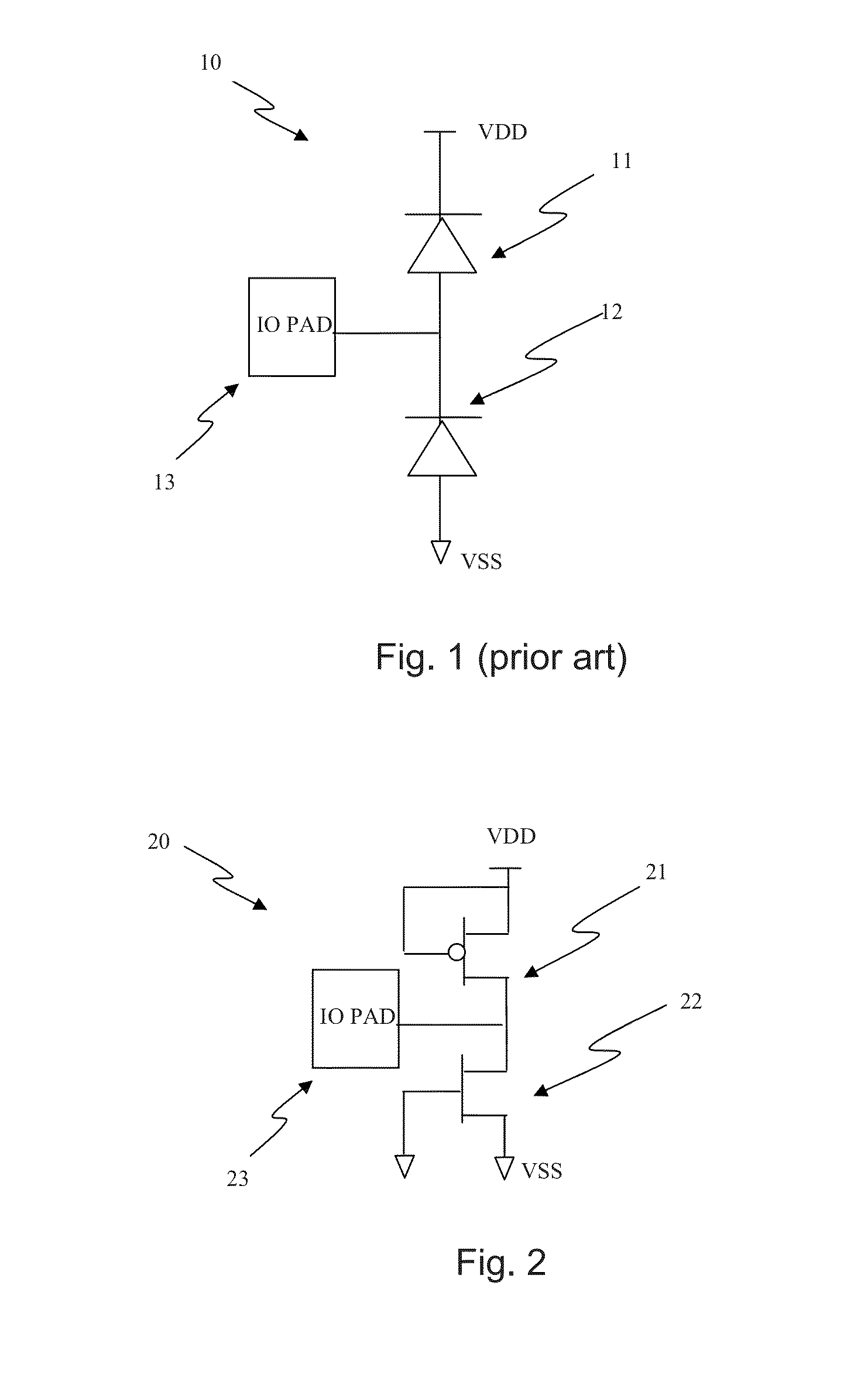
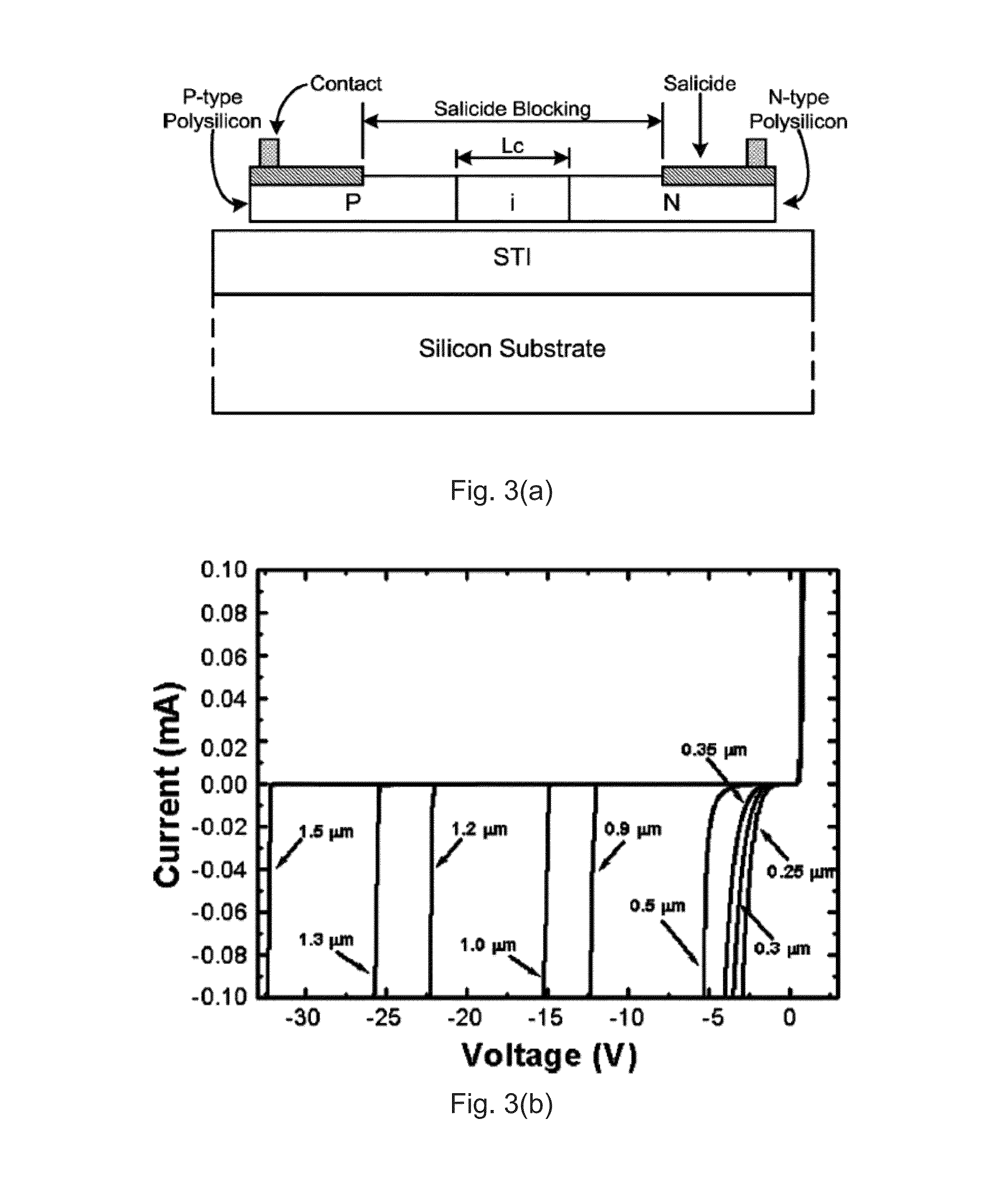
[0045]Embodiments disclosed herein use an ESD structure having a mesh structure of cells with at least one diode on at least one side of at least one cell. The contours of the cells in the mesh can be circle, rectangle, square, triangle, hexagon, or other shapes with polysilicon, active-region, or junction diodes built on at least one side. The diodes can comprise P+ and N+ implants on a polysilicon, active region on an insulated substrate or junction diodes on a silicon substrate. The P+ and N+ implants regions can be separated by a gap (or isolation), such as LOCOS (LOCall Oxidation), STI (Shallow Trench Isolation), dummy gate, or silicide block layer (SBL). The gap can be covered by a silicide block layer (SBL) and overlapping into at least a portion of both P+ and N+ implant areas to form P / N junctions on the insulated or silicon substrate. The diodes can also be constructed from junction diodes with at least one N+ active region on a P substrate or at least one P+ active region...


PUM


Abstract

An Electro-Static Discharge (ESD) protection using at least one I/O pad with at least one mesh structure of diodes provided on a semiconductor body is disclosed. The mesh structure has a plurality of cells. At least one cell can have a first type of implant surrounded by at least one cell with a second type of implant in at least one side of the cell, and at least cell can have a second type of implant surrounded by at least one cell with a first type of implant in at least one side of the cell. The two types of implant regions can be separated with a gap. A silicide block layer (SBL) can cover the gap and overlap into the both implant regions to construct P/N junctions on the polysilicon or active-region body on an insulated substrate. Alternatively, the two types of implant regions can be isolated by LOCOS, STI, dummy gate, or SBL on silicon substrate. The regions with the first and the second type of implants can be coupled to serve as the first and second terminal of a diode, respectively. The mesh structure can have a first terminal coupled to the I/O pad and a first terminal coupled to a first supply voltage.

Description

CROSS-REFERENCE TO RELATED APPLICATIONS[0001]This application claims priority benefit of U.S. Provisional Patent Application No. 61 / 560,173, filed on Nov. 15, 2011 and entitled “Using Mesh-Structure of Polysilicon Diodes for Electro-Static Discharge (ESD) Protection,” which is hereby incorporated herein by reference.BACKGROUND OF THE INVENTION[0002]1. Field of the Invention[0003]The present invention relates to Electro-Static Discharge (ESD) protection, i.e. using mechanism, device, circuit, apparatus, or any means to protection an integrated circuit from ESD damages.[0004]2. Description of the Related Art[0005]Human bodies may carry a lot of electrostatic charges. When an integrated circuit is touched by a human bodies during handling, a very high voltage (˜5KV) and a high current (˜2 A) may be generated that can damage a delicate integrated circuit. The high voltage generated may breakdown MOS gate oxides, and the high power generated by high current may damage the metallurgical j...

Claims


Application Information

Patent Timeline
Patent Type & Authority Applications(United States)
IPC IPC(8): H01L23/60H02H9/04
CPCH02H9/04H01L23/60H01L27/0251H01L27/0296H01L29/735H01L29/868H01L29/0692H01L29/16
Inventor CHUNG, SHINE C.
Owner ATTOPSEMI TECH CO LTD
Why Eureka
Try Eureka