Eureka AIR delivers breakthrough ideas for toughest innovation challenges, trusted by R&D personnel around the world.

Array Substrate and Display Device

Active Publication Date: 2015-12-10
BOE TECH GRP CO LTD
View PDF2 Cites 1 Cited by
  • Summary
  • Abstract
  • Description
  • Claims
  • Application Information

AI Technical Summary

Benefits of technology

The patent text discusses the issue of an offset in the voltage of a display due to feed-in characteristics. The main factor affecting this offset is the gate-source capacitance, which is caused by the overlapping between the gate layer and the source layer. To maintain stability, it is important to control this capacitance by changing the dielectric constant or the distance between the parallel plates. The technical effect of this patent is to provide a solution for controlling the stability of the display's voltage and reducing the offset.

Problems solved by technology

Thus, for each pixel, the common electrode voltage Vcom is not stable, which can cause crosstalk at the time of displaying.

Method used


Image

  • Array Substrate and Display Device
  • Array Substrate and Display Device
  • Array Substrate and Display Device

Examples


Embodiment Construction

[0022]In order to make objects, technical details and advantages of the embodiments of the invention apparent, the technical solutions of the embodiment will be described in a clearly and fully understandable way in connection with the drawings related to the embodiments of the invention. It is obvious that the described embodiments are just a part but not all of the embodiments of the invention. Based on the described embodiments herein, those skilled in the art can obtain other embodiment(s), without any inventive work, which should be within the scope of the invention.

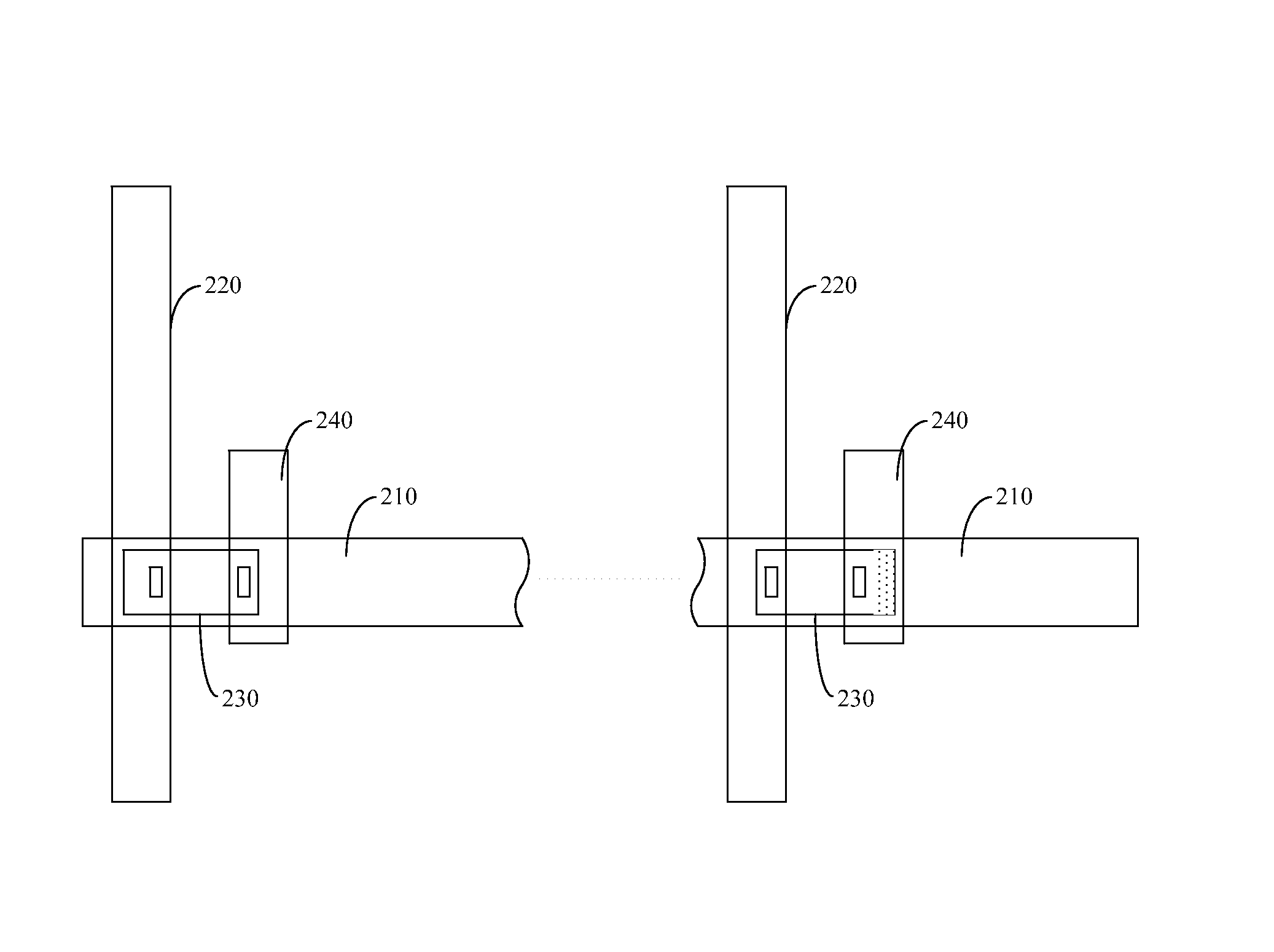
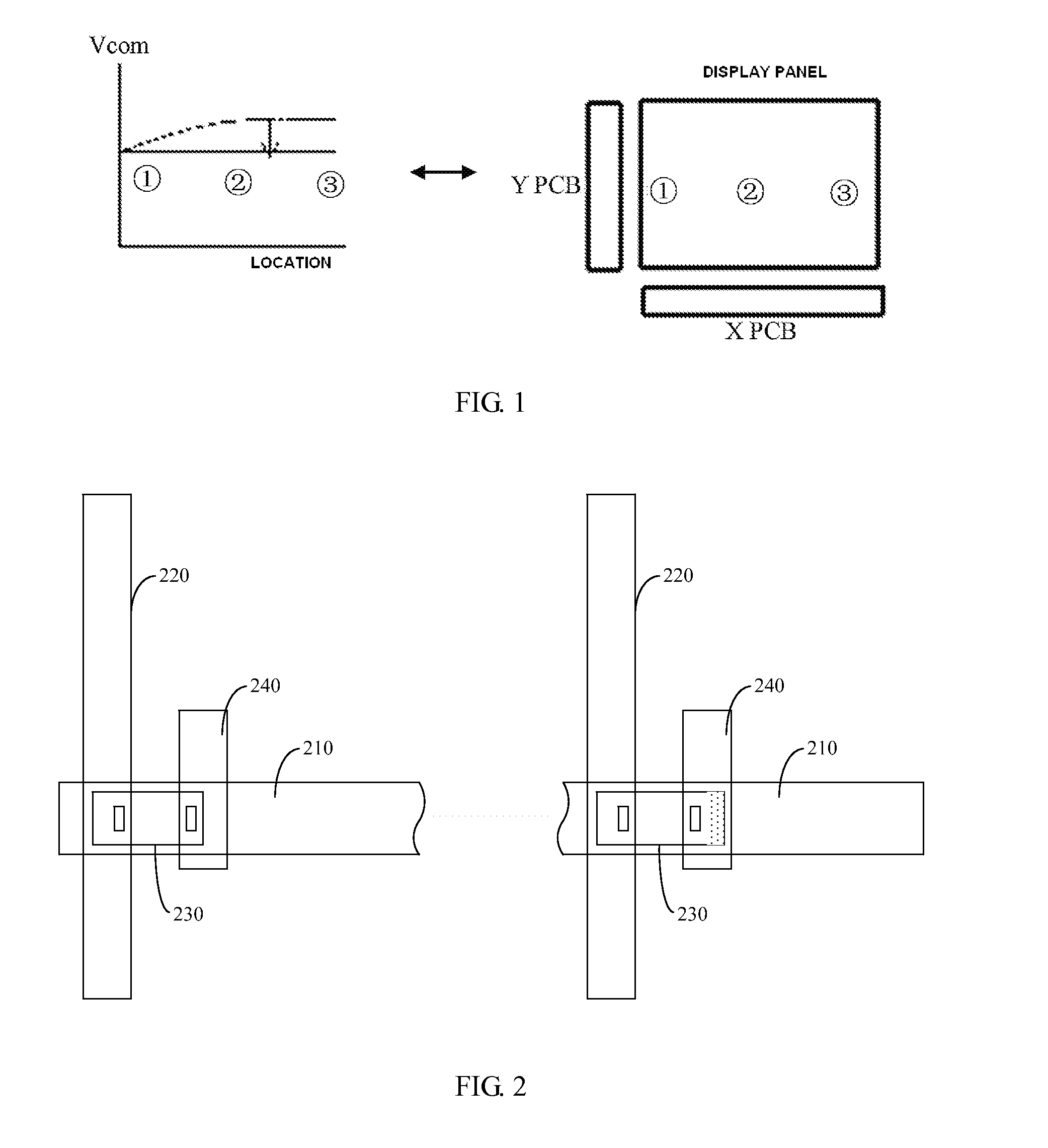
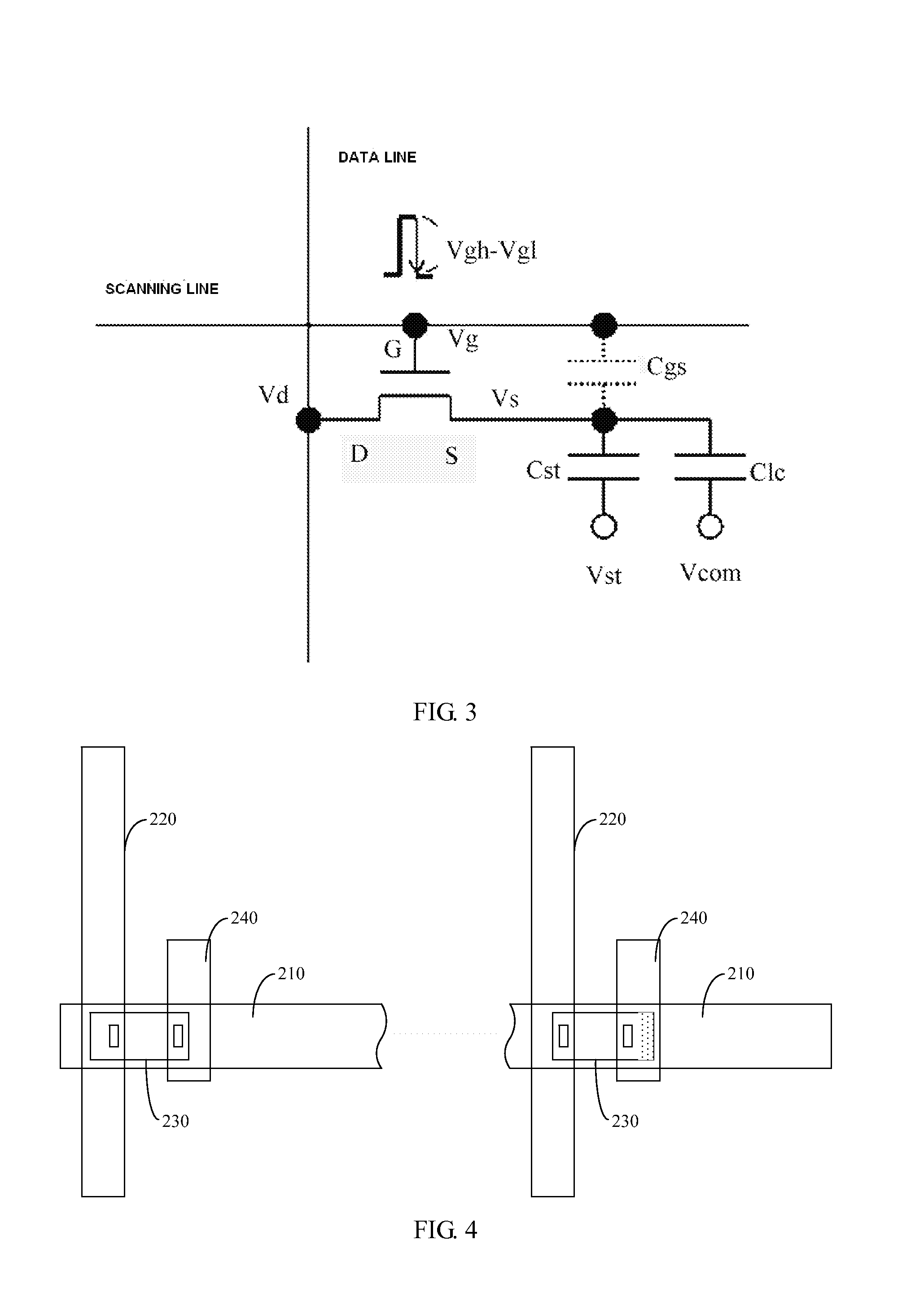
[0023]An array substrate according to an embodiment of present invention, comprises a gate line 210, a data line 220 and a plurality of pixel units defined by the gate line and the data line intersecting with each other, which are formed on a base substrate, and each pixel unit includes a thin film transistor. The plurality of pixel units are arranged in matrix along a row direction and a column direction. One side ...


PUM


Abstract

An array substrate includes a gate line, a data line and a plurality of pixel units defined by the gate line and the data line intersecting with each other, which are formed on a base substrate, and each pixel unit includes a thin film transistor. The farther the thin film transistor is away from a gate driver side of the array substrate, the more likely an overlapping area between an active layer and a source electrode of the thin film transistor shows an increasing trend. By changing the overlapping area between the active layer and the source electrode, a dielectric constant between a gate electrode and the source electrode increases to enlarge a gate-source capacitance Cgs, leading to an increase of ΔVp; as a result, a common electrode voltage tends to be stable, thus avoiding crosstalk at the time of displaying.

Description

TECHNICAL FIELD[0001]Embodiments of the invention relate to an array substrate and a display device.BACKGROUND[0002]Due to a size of a display panel, gate delays (also referred to as RC delay) in different positions are different, so a common electrode voltage Vcom is different in different locations. As illustrated in FIG. 1, the farther a gate line is away from a gate driver (Y PCB in the diagram), the greater the gate delay is; the common electrode voltage Vcom at point {circle around (2)} is greater than that at point {circle around (1)}, that is, the farther the gate line is from the gate driver, the larger the common electrode voltage Vcom will be. Thus, for each pixel, the common electrode voltage Vcom is not stable, which can cause crosstalk at the time of displaying. Actually, Vcom=−ΔVp, where ΔVp is a transition voltage of a pixel voltage Vp caused by a disconnection of the gate line, and V is a common voltage of an actual input; it can be seen that ΔVp could be increased ...

Claims


Application Information

Patent Timeline
IPC IPC(8): H01L27/12
CPCH01L27/1225H01L27/124G02F1/1368H01L27/1222
Inventor NAGAYAMA, KAZUYOSHI
Owner BOE TECH GRP CO LTD
Why Eureka
Eureka Blog
Learn More