Scanning near-field photoacoustic microscopic imager

A photoacoustic microscopy and scanning near-field technology, which is applied to instruments, scientific instruments, and material analysis through optical means, can solve the problems of inability to obtain high resolution, inability to characterize the surface structure of materials and devices, and inability to distinguish materials and devices Problems such as structure and physical properties, to achieve the effect of rich information and high-resolution non-destructive characterization

Inactive Publication Date: 2019-09-20
TONGJI UNIV +1
View PDF7 Cites 4 Cited by
  • Summary
  • Abstract
  • Description
  • Claims
  • Application Information

AI Technical Summary

Problems solved by technology

[0002] Advanced functional materials and devices such as two-dimensional topological materials, thin-film materials, nano-batteries, and multi-layer nano-chips are in the upsurge of research and development. The fields of integrated circuits, new materials, and precision medicine have become national strategic needs. At the nanoscale, there are such Super-resolution surface structure imaging technologies such as AFM, SEM, and SNOM, but currently existing high-resolution detection imaging techniques, such as near-field optical microscopy, use near-field imaging technology to characterize materials and devices at nanometer resolution. Surface structure, but the internal structure and physical properties of materials and devices cannot be distinguished. Although pure acoustic detection can obtain the density and elastic properties of materials, it cannot obtain high resolution at the nanometer level—physical and structural properties at subsurface nanometer resolution. In situ simultaneous non-destructive imaging and characterization technology is still blank
[0005] For example, Chinese patent CN 107589278 A discloses a reflective polarization-modulated near-field scanning optical microscope system based on a fiber optic probe. The disadvantage of this system is that it can only realize scanning near-field imaging of the sample and lacks internal structure information of the sample; Chinese patent CN 107837069 A discloses a photoacoustic microscopic imaging system and method. This system can realize photoacoustic microscopic imaging of the sample to be tested with micron-level resolution, but cannot obtain nanometer-level high resolution. Ratio-dependent characterization of surface structures of materials and devices

Method used


Image

  • Scanning near-field photoacoustic microscopic imager
  • Scanning near-field photoacoustic microscopic imager
  • Scanning near-field photoacoustic microscopic imager

Examples


Embodiment

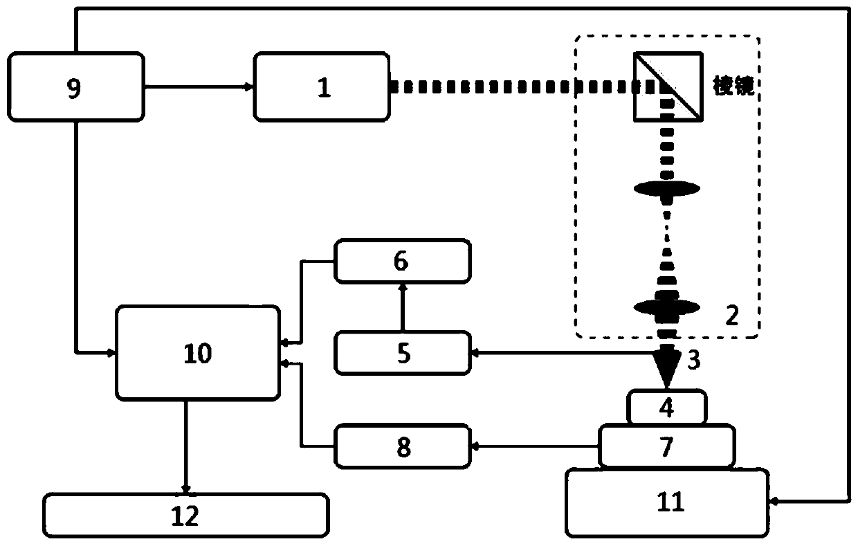
[0036] like figure 1 As shown, the present invention provides a scanning near-field photoacoustic microscopic imager. Near-field optical imaging can characterize the surface structure of materials and devices at nanometer resolution. The near-field optical probe is used to provide a pulsed light source with nanometer resolution. Photoacoustic signals with nanometer resolution can be obtained, and characteristic information such as the structure, optics, heat, mechanics, electricity, and molecular bonds of substances can be obtained through photoacoustic microscopic imaging.

[0037] Specifically, the imager includes:

[0038] Light emitting module: the light source 1 emits light pulses, which are coupled into the near-field optical probe 3 through the optical path collimation and focusing subsystem 2, and then incident on the sample 4;

[0039] Near-field light receiving module: receive and collect the reflected light signal of sample 4;

[0040] Ultrasonic receiving module:...


PUM


Abstract

The invention relates to a scanning near-field photoacoustic microscopic imager, which is used for realizing near-field optics and photoacoustic simultaneous and real-time detection. The scanning near-field photoacoustic microscopic imager comprises a light emitting module, a signal acquisition system, a scanning control module, a timing control module and a signal analysis imaging module, wherein the light emitting module comprises a multi-wavelength pulsed light source, an optical path collimation and focusing subsystem and a near-field optical probe which are arranged in sequence along an optical path; the signal acquisition system comprises a near-field light receiving module, an ultrasonic receiving module and a signal acquisition subsystem; the scanning control module is used for enabling light pulses to move on a sample surface to realize scanning; the timing control module is used for synchronously controlling the pulsed light source to emit the light pulses, the near-field optical probe to receive a light signal, the ultrasonic receiving module to receive a photoacoustic signal and the scanning control module to perform scanning synchronously; and the signal analysis imaging module is used for acquiring a near-field optical image of the sample surface and a near-field photoacoustic image inside the sample. Compared with the prior art, the scanning near-field photoacoustic microscopic imager has the advantages of being capable of near-field optics and photoacoustic simultaneous and real-time detection, being rich in information, satisfying various needs and the like.

Description

technical field [0001] The invention relates to the field of high-resolution surface structure and subsurface physical characteristic detection, in particular to a scanning near-field photoacoustic microscope imager. Background technique [0002] Advanced functional materials and devices such as two-dimensional topological materials, thin-film materials, nano-batteries, and multi-layer nano-chips are in the upsurge of research and development. The fields of integrated circuits, new materials, and precision medicine have become national strategic needs. At the nanoscale, there are such Super-resolution surface structure imaging technologies such as AFM, SEM, and SNOM, but currently existing high-resolution detection imaging techniques, such as near-field optical microscopy, use near-field imaging technology to characterize materials and devices at nanometer resolution. Surface structure, but the internal structure and physical properties of materials and devices cannot be dis...

Claims


Application Information

Patent Timeline
Patent Type & Authority Applications(China)
IPC IPC(8): G01N21/17G01N29/06G01N29/24
CPCG01N21/1702G01N29/0681G01N29/2418G01N2021/1706
Inventor 程茜詹其文解维娅张梦娇陈盈娜张浩南吴诗颖高雅陈一铭
Owner TONGJI UNIV
Why Eureka
Try Eureka