Wafer processing method
A processing method and wafer technology, applied in the manufacture of electrical components, electrical solid devices, semiconductor/solid devices, etc., can solve problems such as transfer between processes that cannot be used, pick-up and lamination damage, large warping deformation, etc., to achieve Reduce the risk of fragmentation, improve stress distribution, and reduce the effect of internal stress
- Summary
- Abstract
- Description
- Claims
- Application Information
AI Technical Summary
Problems solved by technology
Method used
Image

Examples
Embodiment 1
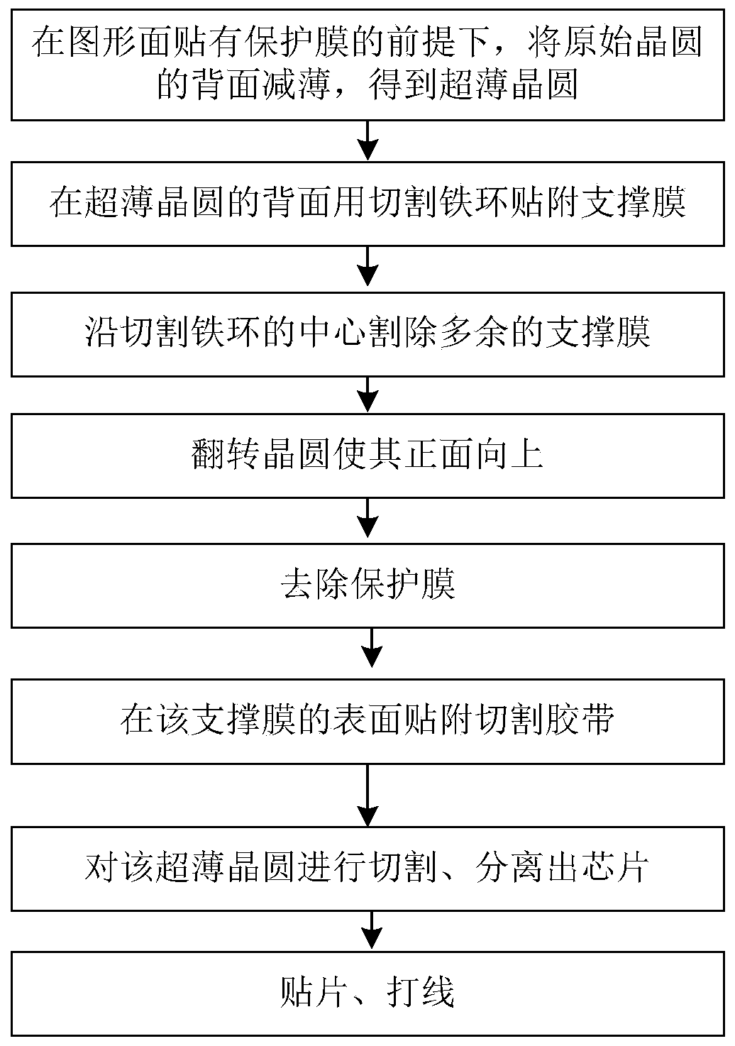
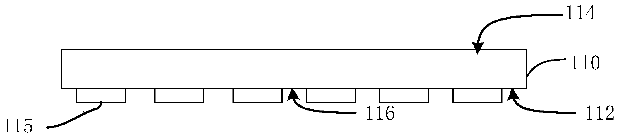
[0055] (1) Thinning the wafer by grinding the back side of the original wafer: adopting a fully automatic grinding and polishing machine that is DISCO DGP8761 with the ability to process wafers of 12 inches and below; The 12-inch raw wafer 110 is ground and polished to obtain an ultra-thin wafer 111 with a thickness of 15 μm.
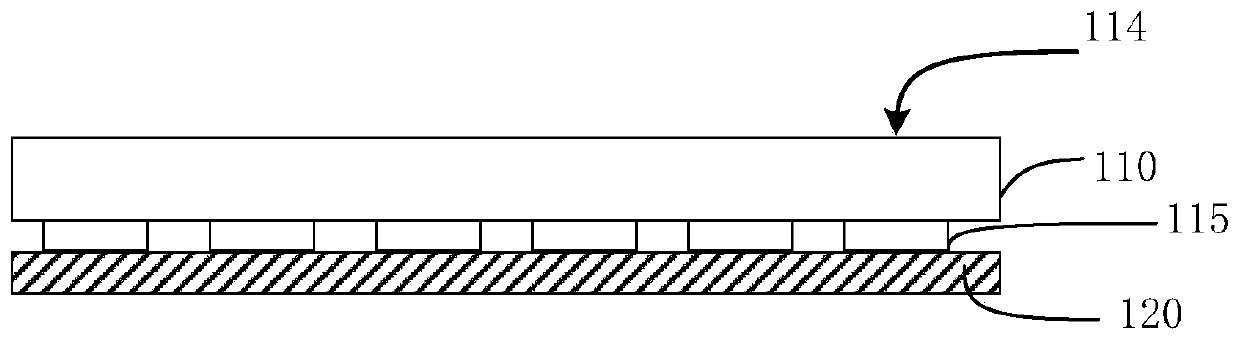
[0056] (2) The support film 130 is pasted on the back surface 114 of the ultra-thin wafer 111 after grinding by using the dicing iron ring 140 . The support film 130 includes an organic film layer 132 made of polyimide, an adhesive layer 134 and a release film layer 136. The release film layer 136 is torn off during the stretching process. After the stretching is completed, the ultra-thin wafer The back surface 114 of the circle 111 is pasted with the adhesive layer 134 of the supporting film 130 and the organic film layer 132 . The material of the organic film layer 132 is polyimide.
[0057] (3) Cut off the redundant supporting film 130 along the ce...
Embodiment 2
[0063] (1) Thinning the wafer by grinding the back side of the original wafer: using a fully automatic grinding and polishing machine that is ACCRETECH PG3000RMX with the ability to process wafers of 12 inches and below, the graphic surface 112 is pasted with a protective film 120 The 8-inch raw wafer 110 is ground and polished to obtain an ultra-thin wafer 111 with a thickness of 20 μm.
[0064] (2) The support film 130 is pasted on the back surface 114 of the ultra-thin wafer 111 after grinding by using the dicing iron ring 140 . The support film 130 includes an organic film layer 132 made of polyimide, an adhesive layer 134 and a release film layer 136. The release film layer 136 is torn off during the stretching process. After the stretching is completed, the ultra-thin wafer The back surface 114 of the circle 111 is pasted with the adhesive layer 134 of the supporting film 130 and the organic film layer 132 . The material of the organic film layer 132 is polyimide.
[0...
Embodiment 3
[0071] (1) Thinning the wafer by grinding the back side of the original wafer: adopting a fully automatic grinding and polishing machine that is DISCO DGP8761 with the ability to process wafers of 12 inches and below; The 8-inch raw wafer 110 is ground and polished to obtain an ultra-thin wafer 111 with a thickness of 35 μm.
[0072] (2) The support film 130 is pasted on the back surface 114 of the ultra-thin wafer 111 after grinding by using the dicing iron ring 140 . The support film 130 includes an organic film layer 132 made of polyimide, an adhesive layer 134 and a release film layer 136. The release film layer 136 is torn off during the stretching process. After the stretching is completed, the ultra-thin wafer The back surface 114 of the circle 111 is pasted with the adhesive layer 134 of the supporting film 130 and the organic film layer 132 . The material of the organic film layer 132 is polyimide.
[0073] (3) Cut off the redundant supporting film 130 along the cen...
PUM
 Abstract
Description
Claims
Application Information
 - R&D
- Intellectual Property
- Life Sciences
- Materials
- Tech Scout
- Unparalleled Data Quality
- Higher Quality Content
- 60% Fewer Hallucinations
Browse by: Latest US Patents, China's latest patents, Technical Efficacy Thesaurus, Application Domain, Technology Topic, Popular Technical Reports.
© 2025 PatSnap. All rights reserved.Legal|Privacy policy|Modern Slavery Act Transparency Statement|Sitemap|About US| Contact US: help@patsnap.com