Ink screen printing process for thick copper white solder resist ink pcb board

A technology of solder resist ink and PCB board, which is applied in the direction of printed circuit, printed circuit manufacturing, and secondary treatment of printed circuit, etc. The effects of white oil cracks, shortening the standing time, and reducing the cost of silk screen printing

Active Publication Date: 2022-03-18
惠州市联达金电子有限公司
View PDF7 Cites 0 Cited by
  • Summary
  • Abstract
  • Description
  • Claims
  • Application Information

AI Technical Summary

Problems solved by technology

[0004] At present, there are many kinds of white solder resist inks used in the market, and the content of titanium dioxide in the existing white solder resist inks is relatively high
Titanium dioxide is an inorganic compound, which is relatively brittle and does not have the flexibility of resin
Therefore, printing the insulating layer of thick copper PCB board with white solder resist ink usually has the following defects: (1) printing the insulating layer of thick copper PCB board with white solder resist ink needs to be printed multiple times, that is, it is cured after one screen printing and then screen printed for the second time. Second, this operation is prone to poor bonding of the interlayer ink, and is prone to delamination and cracking; (2) In the process of mold forming processing, ink cracking often occurs; (3) Reflow soldering or White oil cracks are prone to appear after wave soldering

Method used


Image

  • Ink screen printing process for thick copper white solder resist ink pcb board
  • Ink screen printing process for thick copper white solder resist ink pcb board
  • Ink screen printing process for thick copper white solder resist ink pcb board

Examples


Embodiment 1

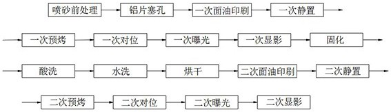
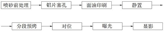
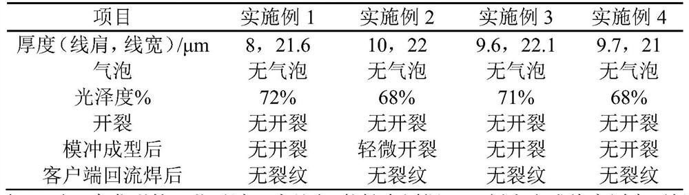
[0042]For the thick copper PCB board with a total copper thickness of 128 μm, the white solder resist ink layer is screen-printed, and the specific steps are as follows:

[0043] S1. Perform sandblasting pre-treatment on the thick copper PCB board to be screen-printed with solder resist ink, and use aluminum sheets to plug the via holes.

[0044] S2. Use 36T screen printing mesh to print white solder resist ink. Among them, the printing uses a new squeegee at 75 degrees. In addition, the white solder resist ink is used after oiling. Specifically, after oiling, stir for 17 minutes and let it stand for 30 minutes, so that the viscosity of the white solder resist ink reaches 200dpa.s, and then use it for printing.

[0045] Moreover, the angle of the screen printing squeegee for printing is 26°, and the air pressure of the screen printing is 6.2kg / cm 2 , the screen printing speed is 2.2m / min; and after the screen printing is completed, the screen frame rises, and the ink on the ...

Embodiment 2

[0050] For the thick copper PCB with a total copper thickness of 116 μm, the white solder resist ink layer is screen-printed, and the specific steps are as follows:

[0051] S1. Perform sandblasting pre-treatment on the thick copper PCB board to be screen-printed with solder resist ink, and use aluminum sheets to plug the via holes.

[0052] S2. Use 36T screen printing mesh to print white solder resist ink. Among them, the printing uses a new squeegee at 75 degrees. In addition, the white solder resist ink is used after oiling. Specifically, after oiling, stir for 20 minutes and let it stand for 30 minutes to make the viscosity of the white solder resist ink reach 185dpa.s, and then use it for printing.

[0053] Moreover, the angle of the screen printing squeegee for printing is 23°, and the air pressure of the screen printing is 6.1kg / cm 2 , the screen printing speed is 2.2m / min; and after the screen printing is completed, the screen frame rises, and the ink on the screen f...

Embodiment 3

[0058] For the thick copper PCB with a total copper thickness of 140 μm, the white solder resist ink layer is screen-printed, and the specific steps are as follows:

[0059] S1. Perform sandblasting pre-treatment on the thick copper PCB board to be screen-printed with solder resist ink, and use aluminum sheets to plug the via holes.

[0060] S2. Use 36T screen printing mesh to print white solder resist ink. Among them, the printing uses a new squeegee at 75 degrees. In addition, the white solder resist ink is used after oiling. Specifically, after oiling, stir for 15 minutes and then let it stand for 30 minutes, so that the viscosity of the white solder resist ink reaches 180dpa.s, and then use it for printing.

[0061] Moreover, the angle of the screen printing squeegee for printing is 24°, and the air pressure of the screen printing is 6.5kg / cm 2 , the screen printing speed is 2.5m / min; and after the screen printing is completed, the screen frame rises, and the ink on the ...


PUM

PropertyMeasurementUnit
thicknessaaaaaaaaaa
thicknessaaaaaaaaaa
thicknessaaaaaaaaaa

Abstract

The invention discloses an ink screen printing process for a thick copper white solder resist ink PCB board. The silk screen printing process includes the following steps: S1, performing pre-sandblasting treatment on the thick copper PCB board to be screen-printed with solder resist ink, and performing plugging treatment on the via holes; S2, using screen printing white solder resist ink, and standing still; S3. Segmented pre-baking, alignment, exposure and development are carried out sequentially to complete the ink screen printing. The process of the present invention can complete the white solder resist ink layer with a shoulder thickness of not less than 7 μm on the thick copper PCB board through one silk screen printing, which improves the efficiency of silk screen printing, reduces the cost of silk screen printing, and avoids the ink layer being stamped during die punching. easy cracking; and through segmental pre-baking, not only shortens the standing time after silk screen printing, but also solves the defect of white oil cracks; at the same time, by controlling the energy of exposure and development, the ink layer maintains gloss, development is clear, and It effectively avoids the shortcoming that white oil cracks are prone to appear after reflow soldering or wave soldering on the client side.

Description

technical field [0001] The invention relates to the technical field of production of thick copper PCB boards, in particular to an ink screen printing process for thick copper white solder resist ink PCB boards. Background technique [0002] With the development of LED (Light-Emitting Diode, light-emitting diode) lamps, lamps and outdoor and indoor billboards basically replace traditional tungsten lamps with LED lamps. At the same time, LED lamps are widely used in roads, homes, automobiles, advertising decoration, and civil, industrial, medical, aerospace, and military industries. [0003] The PCB board (Printed Circuit Board, printed circuit board) on the LED lamps generally uses white solder resist ink as the insulating layer of the lamps. This is because the white ink has the characteristics of high reflective efficiency, which can greatly reduce the loss of light. This enables the lamps to obtain better illuminance under the same conditions. PCB boards use white solder...

Claims


Application Information

Patent Timeline
Patent Type & Authority Patents(China)
IPC IPC(8): H05K3/28
CPCH05K3/282
Inventor 杨展仁
Owner 惠州市联达金电子有限公司
Why Eureka
Try Eureka