Air bridge integrated inductor and manufacturing method thereof

A technology integrating inductors and manufacturing methods, which is applied in the direction of inductors, circuits, electrical components, etc., and can solve problems such as the decrease of the Q value of the inductor, the reduction of the magnetic flux of the inductor coil, and the large energy loss.

Active Publication Date: 2019-09-24
福建省福联集成电路有限公司
View PDF6 Cites 2 Cited by
  • Summary
  • Abstract
  • Description
  • Claims
  • Application Information

AI Technical Summary

Problems solved by technology

[0002] In the prior art, most integrated inductors with a planar structure are used. Since this integrated inductor is fabricated on a plane parallel to the substrate, under high-frequency conditions, an eddy current (Eddy Current) will be formed in the substrate, and the eddy current The direction is opposite to the direction of the current in the inductor coil,

Method used


Image

  • Air bridge integrated inductor and manufacturing method thereof
  • Air bridge integrated inductor and manufacturing method thereof
  • Air bridge integrated inductor and manufacturing method thereof

Examples


Embodiment Construction

[0042] In order to explain in detail the technical content, structural features, achieved goals and effects of the technical solution, the following will be described in detail in conjunction with specific embodiments and accompanying drawings.

[0043] see Figure 1 to Figure 11 , This embodiment provides a method for preparing an air bridge integrated inductor, which is used on a wafer, which can reduce the occupation of the surface area of ​​the wafer, improve the integration degree of the chip, and reduce the production cost of the chip.

[0044] The present invention comprises the steps:

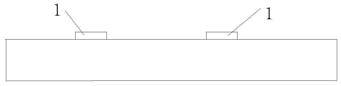
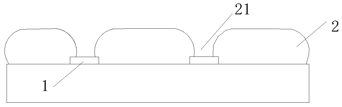
[0045] Fabricating the first inductive metal layer 1 by evaporation on the substrate; Figure 11 Among them, AE, BF, CG, DH, I, and J are all the first inductive metal layers; among them, AE, BF, CG, and DH are parallel laminate structures.

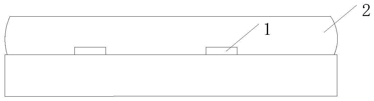
[0046] Fabricate the first layer of photoresist 2 on the first inductive metal layer 1, etch the pier position of the air bridge to be made to f...


PUM


Abstract

The invention discloses an air bridge integrated inductor and a manufacturing method thereof. The manufacturing method comprises the steps of manufacturing a first inductive metal layer on a substrate; manufacturing a first layer of photoresist on the first inductive metal layer, and etching the bridge pier position of the air bridge to be manufactured to form a groove; manufacturing a metal connecting layer on the first layer of photoresist and the groove; manufacturing a second layer of photoresist on the metal connecting layer; exposing and developing on the second layer of photoresist, and removing the metal connecting layer on the groove to form an air bridge path; manufacturing a second inductive metal layer on the second layer of photoresist, wherein the second inductive metal layer is connected with the first inductive metal layer at the position of the groove; and removing the first layer of photoresist, the metal connecting layer and the second layer of photoresist. The air bridge integrated inductor takes the second inductive metal layer as main metal to enable an inductance coil to be distributed in a three-dimensional mode, thereby improving the inductive magnetic flux to increase the inductance and reducing the eddy current at the same time, and improving the quality factor Q value and the performance of the inductance coil.

Description

technical field [0001] The invention relates to the technical field of semiconductor manufacturing, in particular to a method for manufacturing an air bridge integrated inductor and the integrated inductor. Background technique [0002] In the prior art, most integrated inductors with a planar structure are used. Since this integrated inductor is fabricated on a plane parallel to the substrate, under high-frequency conditions, an eddy current (Eddy Current) will be formed in the substrate, and the eddy current The direction is opposite to the direction of the current in the inductor coil, which will lead to a decrease in the magnetic flux of the inductor coil, a large additional energy loss and a decrease in the Q value of the entire inductor. In addition, in the prior art, due to the limitations of the manufacturing process and materials of the integrated circuit, it is difficult for the integrated inductor to simultaneously achieve a high inductance value and a high qualit...

Claims


Application Information

Patent Timeline
IPC IPC(8): H01L23/64
CPCH01L28/10
Inventor 林豪林易展陈智广陈建星林张鸿林伟铭
Owner 福建省福联集成电路有限公司
Why Eureka
Try Eureka