Pixel unit circuit, image processing method, storage medium and CMOS image sensor

An image sensor and pixel unit technology, applied in the field of image processing, can solve problems such as reducing the absorption rate of incident light and increasing the size of CMOS image sensors

Active Publication Date: 2019-09-27
GUANGDONG OPPO MOBILE TELECOMM CORP LTD
View PDF8 Cites 3 Cited by
  • Summary
  • Abstract
  • Description
  • Claims
  • Application Information

AI Technical Summary

Problems solved by technology

[0004] However, each pixel unit circuit can only absorb RGB monochromatic light. When it is necessary to obtain RGB combined light corresponding to a black-and-white image, multiple pixel unit circuits are required to absorb RGB monochromatic light, which leads to an increase in the size of the CMOS image sensor, and The absorption rate of incident light is greatly reduced when collecting black and white images

Method used


Image

  • Pixel unit circuit, image processing method, storage medium and CMOS image sensor
  • Pixel unit circuit, image processing method, storage medium and CMOS image sensor
  • Pixel unit circuit, image processing method, storage medium and CMOS image sensor

Examples


Embodiment 1

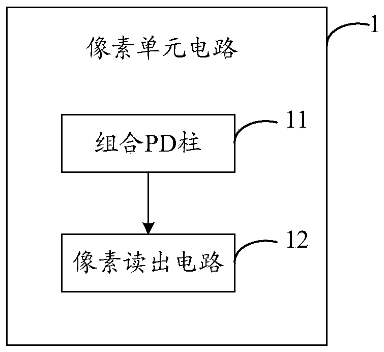
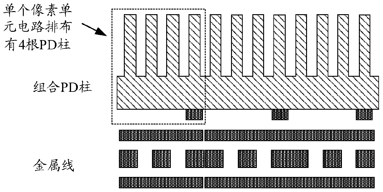
[0049] An embodiment of the present application provides a pixel unit circuit, which is applied to a CMOS image sensor, such as figure 1 As shown, the pixel unit circuit includes:

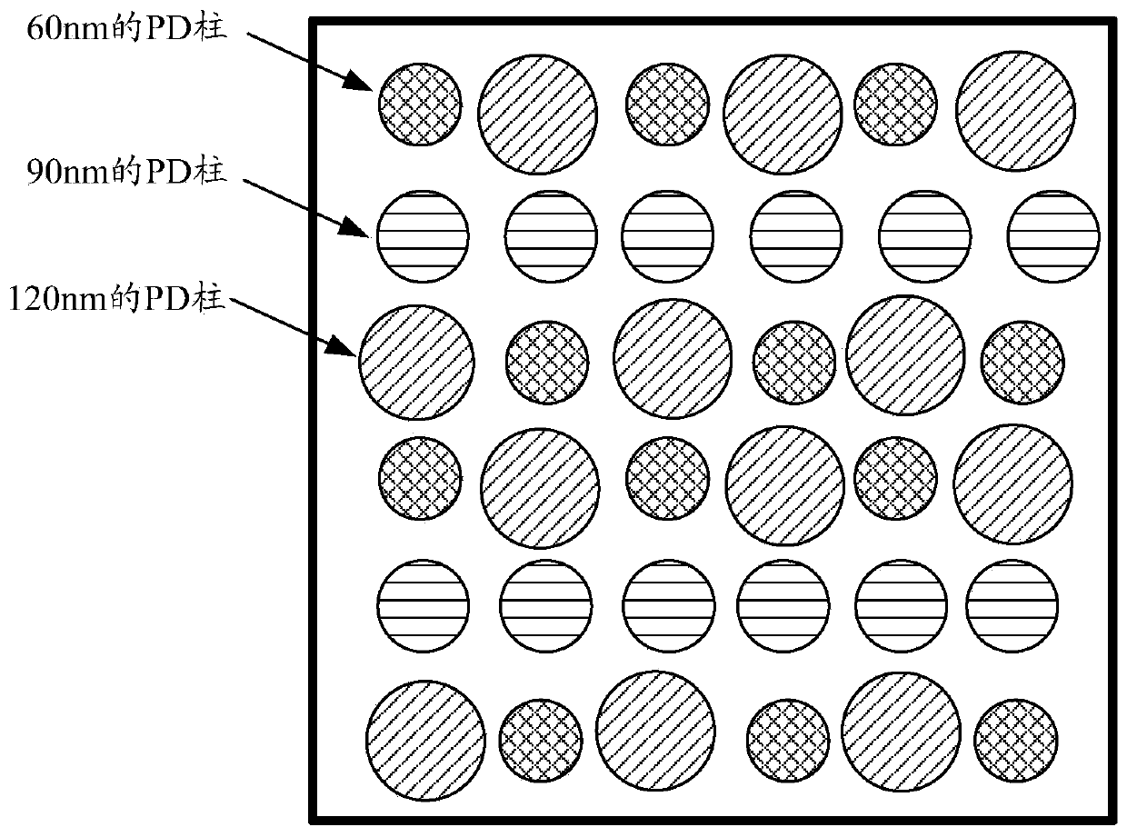
[0050] A combined PD column composed of photodiodes PD with at least two preset diameters is used to absorb RGB combined optical signals of at least two preset wavelength bands by using the PD columns with at least two preset diameters, and convert the RGB The combined optical signal is converted into a combined electrical signal; the number of PD columns with a preset diameter among the at least two preset diameters of PD columns is a preset number;

[0051] The pixel readout circuit connected to the combined PD column is used to amplify the combined electrical signal and read out the combined electrical signal.

[0052] The pixel unit circuit provided by the embodiment of the present application is applicable to a scenario where a CMOS image sensor is used to process an image of an absorbed ligh...

Embodiment 2

[0095] An embodiment of the present application provides an image processing method, which is applied to a CMOS image sensor composed of a pixel unit circuit. The pixel unit circuit includes a combined PD column composed of at least two PD columns with preset diameters and a pixel connected to the combined PD column. readout circuits such as Figure 5 As shown, the method includes:

[0096] S101. Using PD columns with at least two preset diameters to respectively absorb RGB combined optical signals of at least two preset wavelength bands, and convert the RGB combined optical signals into combined electrical signals;

[0097] The pixel unit circuit provided by the embodiment of the present application is applicable to a scenario where a CMOS image sensor is used to process an image of an absorbed light signal to obtain an image corresponding to the light signal.

[0098] In the embodiment of the present application, the CMOS image sensor is composed of a pixel unit circuit and...

Embodiment 3

[0134] An embodiment of the present application provides a storage medium on which a computer program is stored. The computer-readable storage medium stores one or more programs. The one or more programs can be executed by one or more processors and applied to pixel In the unit circuit, the computer program realizes the image processing method described in the second embodiment.

[0135] Specifically, when the program instructions corresponding to an image processing method in this embodiment are read or executed by an electronic device, the following steps are included:

[0136] Using the PD columns with at least two preset diameters to respectively absorb RGB combined optical signals of at least two preset wavelength bands, and convert the RGB combined optical signals into combined electrical signals;

[0137] The combined electrical signal is amplified, and the combined electrical signal is read out.

[0138] In an embodiment of the present application, further, the at lea...


PUM


Abstract

The embodiment of the invention discloses a pixel unit circuit, an image processing method, a storage medium and a CMOS image sensor. The circuit is applied to CMOS image sensor, the pixel unit circuit comprises: a combined PD column composed of at least two photodiode PD columns with preset diameters, wherein the combined PD column is used for absorbing RGB combined optical signals of at least two preset wavebands through the at least two PD columns with the preset diameters and converting the RGB combined optical signals into combined electric signals, and the number of the PD columns with one preset diameter in the at least two PD columns with the preset diameters is the preset number; and a pixel reading circuit which is connected with the combined PD column and is used for amplifying the combined electric signal and reading the combined electric signal.

Description

technical field [0001] The present application relates to the field of image processing, in particular to a pixel unit circuit, an image processing method, a storage medium, and a CMOS image sensor. Background technique [0002] In recent years, image sensors have been widely used in the field of image processing, and image sensors include: Charged Coupled Device (CCD) image sensors and Complementary Metal Oxide Semiconductor (Complementary Metal Oxide Semiconductor, CMOS) image sensors , Compared with CCD image sensors, CMOS image sensors are more widely used due to their high sensitivity and fast output capabilities. [0003] In the existing CMOS image sensor, each pixel unit circuit includes a photodiode (PD) structure, and the PD structure is used to absorb RGB monochromatic light. When it is necessary to use the CMOS image sensor to obtain a black and white image, it is necessary to use multiple pixels The unit circuit absorbs multiple RGB monochromatic lights. [000...

Claims


Application Information

Patent Timeline
Patent Type & Authority Applications(China)
IPC IPC(8): H04N5/374H04N5/378H01L27/146
CPCH01L27/146H01L27/14643H01L27/14683H01L27/14612H04N25/76H04N25/75
Inventor 杨鑫
Owner GUANGDONG OPPO MOBILE TELECOMM CORP LTD
Why Eureka
Try Eureka