High thermal conductivity wave-absorbing organosilicon composition and preparation method thereof

A technology of organosilicon and composition, applied in the field of high thermal conductivity wave absorbing organosilicon composition and preparation thereof, can solve the problems that the thermal conductivity of the product is difficult to meet the requirements for use, the thickness of the material is difficult to control, and the continuous production is difficult, and it is beneficial to large-scale production. Large-scale continuous production, simple operation, and the effect of improving thermal conductivity

Inactive Publication Date: 2019-10-01
SHENZHEN FRD SCI & TECH
View PDF8 Cites 10 Cited by
  • Summary
  • Abstract
  • Description
  • Claims
  • Application Information

AI Technical Summary

Problems solved by technology

[0003] The existing common solution is to use heat conduction material and shielding wave absorbing material to realize heat conduction and shielding wave absorbing. The biggest disadvantage of this solution is that it is difficult to control the thickness of the overall material and the thermal conductivity of the compounded product is difficult to achieve. Require
[0004] Patent CN108495897A discloses a thermally conductive resin molded product. Under 500KPa, the thermal resistance of the thermally conductive resin sheet is as low as 0.4°Ccm 2 / W, but the patent does not mention the physical properties of the product, electromagnetic shielding and wave-absorbing effects, and its extrudates are difficult to use in continuous production after curing

Method used


Image

  • High thermal conductivity wave-absorbing organosilicon composition and preparation method thereof
  • High thermal conductivity wave-absorbing organosilicon composition and preparation method thereof
  • High thermal conductivity wave-absorbing organosilicon composition and preparation method thereof

Examples


preparation example Construction

[0040] The preparation method of the high thermal conductivity and wave-absorbing silicone composition of the present invention may include the following steps:

[0041] S1. Mix the raw materials in parts by mass to form a mixture.

[0042] S2. Extrude the mixture into a sheet through an extruder.

[0043] Among them, the length of the extrusion cavity of the extruder is 0.5cm-50cm, preferably 2cm-10cm; the length of the extrusion cavity is less than 2cm, the orientation is insufficient, and it is difficult to extrude if the length is greater than 10cm. The width of the extrusion cavity is 0.1mm-50mm. It is preferably 1cm-5cm; the width of the extrusion cavity is less than 1cm, which will result in too small size of the finished product, and it is difficult to extrude a complete sheet if it is greater than 5cm. The thickness of the extrusion cavity is 0.1mm-10mm, preferably 0.3mm-2mm; if the thickness of the extrusion cavity is less than 0.3mm, it will be difficult for the sheet to...

Embodiment 1

[0052] Separately 700g of long-chain polyvinyl-terminated dimethylsiloxane with an average molecular weight of 500,000, 100g of vinyl-terminated dimethylsiloxane with an average molecular weight of 2000, and 200g of polydimethylsiloxane with an average molecular weight of 1000 Silicone was added to a 2L kneader, kneaded and stirred at room temperature for 5 minutes, and then added in batches 1000g of flake graphite powder with an average particle size of 25μm, 500g of carbon-based nickel powder with an average particle size of 3μm, and 500g average particle size. Carbon-based iron powder with a diameter of 2μm, 200g BET specific surface area of ​​200m 2 / g of fumed silica, mixed for 2 hours at room temperature. After mixing, take out 400g and add 2g long-chain polydimethylsiloxane mixture containing 50% 2,5-dimethyl-2,5-di-tert-butylperoxyhexane and an average molecular weight of 500,000. Mix uniformly on an open mill, and extrude through a screw extruder into a sheet with a th...

Embodiment 2

[0054] Respectively, 600g of long-chain polydimethylsiloxane with an average molecular weight of 500,000, 200g of vinyl-terminated dimethylsiloxane with an average molecular weight of 2000, and 200g of polydimethylsiloxane with an average molecular weight of 500 Add to a 2L kneader, knead and stir at room temperature for 5 minutes, and then add 1000g of flake graphite powder with an average particle size of 40μm, 500g of carbon-based nickel powder with an average particle size of 3μm, and 500g with an average particle size of 2μm. Carbon-based iron powder, 200g BET specific surface area of ​​200m 2 / g of fumed silica, mixed for 2 hours at room temperature. After mixing, take out 400g and add 2g long-chain polydimethylsiloxane mixture containing 50% 2,5-dimethyl-2,5-di-tert-butylperoxyhexane and an average molecular weight of 500,000. Mix uniformly on an open mill, and extrude into a 0.6mm thick, 30mm wide and 40cm long sheet through a screw extruder. This kind of sheet is then...


PUM

PropertyMeasurementUnit
particle diameteraaaaaaaaaa
specific surface areaaaaaaaaaaa

Abstract

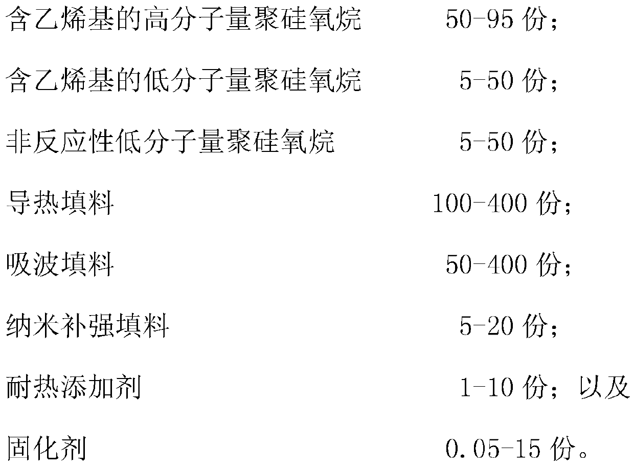
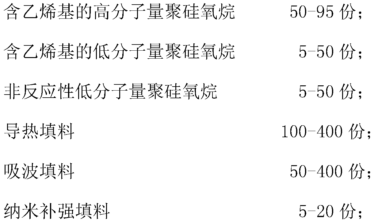
The invention discloses a high thermal conductivity wave-absorbing organosilicon composition and a preparation method thereof. The high thermal conductivity wave-absorbing organosilicon composition isprepared from the following raw materials in parts by mass: 50-95 parts of vinyl-containing high molecular weight polysiloxane, 5-50 parts of vinyl-containing low molecular weight polysiloxane, 5-50parts of non-reactive low molecular weight polysiloxane, 100-400 parts of thermal conductive filler, 50-400 parts of wave-absorbing filler, 5-20 parts of nano reinforcing filler, 1-10 parts of a heat-resistant additive and 0.05-15 parts of a curing agent. The high thermal conductivity wave-absorbing organosilicon composition provided by the invention increases the thermal conductivity by aligningthe sheet-like thermal conductive filler, realizes electromagnetic shielding and wave absorbing of the composition by using the wave-absorbing filler with electromagnetic shielding and wave absorbingeffects, and improves the physical properties of the composition by adding the nano reinforcing filler. The obtained composition has a thermal conductivity greater than 10W / (m.K), a shielding effectiveness greater than 30dB, a tensile strength greater than 0.3MPa and an elongation at break greater than 80%.

Description

Technical field [0001] The present invention relates to the technical field of thermally conductive materials for components, in particular to a high thermal conductivity wave-absorbing organic silicon composition and a preparation method thereof. Background technique [0002] With the continuous development of electronic technology, the size of components is getting smaller and smaller, and the degree of integration is also increasing. They will generate a lot of heat during operation. The accumulation of this heat brings about the service life and reliability of components. Fatal impact. In order to quickly dissipate the heat generated during the operation of the components, a thermally conductive material with higher thermal conductivity must be required to conduct the heat. At the same time, with the application of 5G technology, the noise of electromagnetic waves has become larger and larger. In order to reduce the interference of electromagnetic waves to other components a...

Claims


Application Information

Patent Timeline
Patent Type & Authority Applications(China)
IPC IPC(8): C08L83/07C08L83/04C08K13/06C08K7/00C08K3/04C08K3/08
CPCC08K2003/0856C08K2003/0862C08K2201/003C08K2201/011C08K2201/016C08L83/04C08L2205/025C08L2205/035C08K13/06C08K7/00C08K3/04C08K3/08
Inventor 奚家国陶志伟
Owner SHENZHEN FRD SCI & TECH
Why Eureka
Try Eureka