
A Charge Compensation Circuit and Memory Structure for Reducing Read Operation Voltage Jitter

A charge compensation and voltage jitter technology, applied in the field of memory, can solve the problems of increasing the response speed and driving capacity of the charge pump, difficult to fully recover the VPP voltage, and increasing the VPP ripple, so as to reduce the output capacity requirements and reduce power consumption. , the effect of reducing the area

Active Publication Date: 2021-01-19
合肥联诺科技股份有限公司
View PDF9 Cites 0 Cited by
  • Summary
  • Abstract
  • Description
  • Claims
  • Application Information

AI Technical Summary

Problems solved by technology

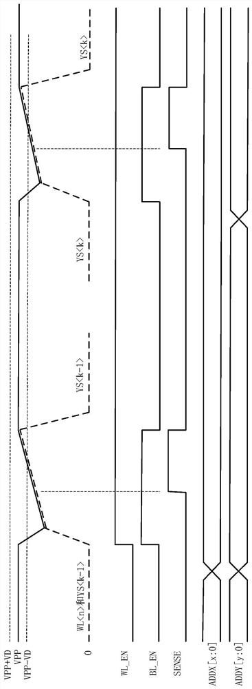
Due to the speed requirements of the read command, the time from WL_EN to SENSE is generally very short, and it is difficult for the VPP voltage to fully recover
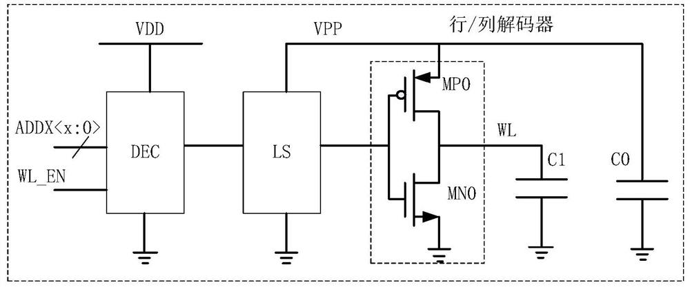
When WL_EN is switched, the voltage drop on VPP can be approximated as C1 / (C1+C0). If C0 is large enough, the voltage drop is very small, which can meet the needs; in fact, for small-capacity memories, C0 is usually small. If you want To meet the requirements of fast recovery of VPP, one method is to add a large number of on-chip capacitors to VPP, which leads to an increase in cost. Another method is to increase the response speed and drive capability of the charge pump, but also increase the area. and will cause the ripple of VPP to increase

Method used


Image

  • A Charge Compensation Circuit and Memory Structure for Reducing Read Operation Voltage Jitter
  • A Charge Compensation Circuit and Memory Structure for Reducing Read Operation Voltage Jitter
  • A Charge Compensation Circuit and Memory Structure for Reducing Read Operation Voltage Jitter

Examples


Embodiment 1

[0022] A charge compensation circuit that reduces voltage jitter in read operations, such as Figure 4 As shown, it is mainly driven by the compensation output of the front end connected to the WL_EN / BL_EN signal (MP1, MN1 is the equivalent drive of the compensation voltage) and the compensation capacitor CX / CY / CY connected to the compensation output drive at the front end and connected to the read voltage VPP at the rear end constitute.

[0023] The compensation output driver outputs a compensation voltage VX / VY, and charges the compensation capacitor CX / CY, thereby compensating the read voltage VPP; VDD provides a high voltage for the compensation output driver.

[0024] Take the row decoding enable signal as an example, when the WL_EN signal is switched from 0 to 1, WL is pulled from 0 to VPP, and the amount of charge extracted by C1 from VPP is C1*VPP; at the same time, CX is connected to the pole on the side of the compensation output drive The plate is pulled up from 0 ...

Embodiment 2

[0029] Considering that there is a certain ripple in VDD, in order to avoid the impact of VDD ripple on VPP during read operation, CX / CY can be disconnected from VDD after performing charge compensation on VPP.

[0030] Therefore, on the basis of Embodiment 1, the front end of the compensation output driver is connected with a gating control circuit, so that the compensation output driver only outputs compensation voltage when WL_EN / BL_EN=1 and SENSE=0.

[0031] The gating control circuit is composed of a gating control signal, a single-stage reverse circuit, and a NAND gate circuit, such as Figure 5 As shown, the gate control signal adopts but is not limited to the SENSE signal, the gate control signal is connected to the single-stage reverse circuit, the single-stage reverse circuit is connected to the NAND gate circuit, and the AND The NOT gate circuit is connected to one input terminal of the compensation output driver, and the WL_EN / BL_EN signal is connected to the other...

Embodiment 3

[0035] A memory structure that reduces voltage jitter for read operations, such as Figure 6 As shown, a first charge compensation circuit and a second charge compensation circuit are respectively connected to the row decoder and the column decoder of the original memory structure, and both the first charge compensation circuit and the second charge compensation circuit are implemented by using The charge compensation circuit described in example 1 or embodiment 2;

[0036] The WL_EN signal of the row decoder is connected to the first charge compensation circuit, and the output terminal of the first charge compensation circuit is connected to the read voltage VPP; the BL_EN signal of the column decoder is connected to the second charge compensation circuit. circuit, the output end of the second charge compensation circuit is connected to the read voltage VPP.

[0037] Figure 7 It is a waveform diagram of the signal voltage during the read operation of the memory provided wi...


PUM


Abstract

The invention discloses a charge compensation circuit for reducing read operation voltage jitter and a memory structure. A row decoder and a column decoder of an original memory structure are respectively connected with a charge compensation circuit, wherein the front end of the compensation output drive is connected with a WL _ EN / BL _ EN signal, the rear end of the compensation capacitor is connected with a compensation output drive, the rear end of the compensation capacitor is connected with a reading voltage VPP, the compensation output drive outputs compensation voltage, the compensationcapacitor is charged, and then the reading voltage VPP is compensated; and the chip power supply VDD provides high voltage for the compensation output drive. According to the invention, the problem that the VPP voltage drop caused by the load capacitor affects the reading operation accuracy is solved; compared with the prior art, the VPP chip has the advantages that the increase of C0 accommodation or the addition of on-chip capacitors is avoided, the chip cost is reduced, and on the contrary, the load capacitance of the VPP is reduced and the voltage recovery is faster by reducing the C0 capacitance value; and meanwhile, the requirement on the output capability of the charge pump is also reduced.

Description

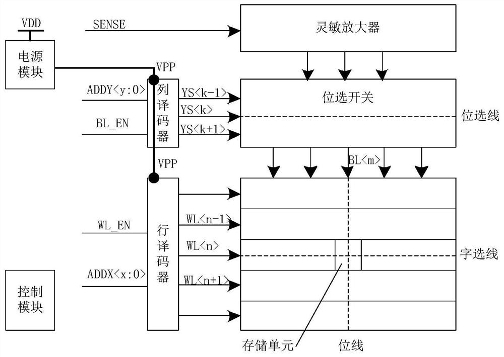
technical field [0001] The invention relates to the technical field of memory, in particular to a charge compensation circuit and a memory structure for reducing read operation voltage jitter. Background technique [0002] Memory is one of the indispensable components in modern electronic products. The internal storage units are usually arranged in a large array. According to the address, the corresponding storage unit is selected by the decoder to complete the internal data read and write operations of the storage unit. , and the stability of the voltage when reading and writing data has a great impact on performance. figure 1 It is a FLASH memory structure among many memories, which includes the following core physical parts: memory cell array, row decoder, column decoder, bit selection switch, sense amplifier, power supply module and control module. [0003] The storage unit is a floating gate field effect transistor. The gates of all storage units in each row are connec...

Claims


Application Information

Patent Timeline
Patent Type & Authority Patents(China)
IPC IPC(8): G11C16/30G11C16/08G11C16/26
CPCG11C16/08G11C16/26G11C16/30
Inventor 胡燕黄纪业
Owner 合肥联诺科技股份有限公司
Learn More