Array chip for cell capture and tumor ball culture and preparation and operation method thereof
A cell culture and tumor sphere technology, applied in the field of array chip preparation, can solve the problems of single cell chip function and single cell waste, and achieve the effects of simple and fast operation, simple and easy preparation method and operation method.
- Summary
- Abstract
- Description
- Claims
- Application Information
AI Technical Summary
Problems solved by technology
Method used
Image

Examples
preparation example Construction
[0051] The method for preparing an arrayed chip for cell capture and tumorsphere culture of the present invention specifically includes the following steps:
[0052] Step 1, prepare single cell sorting layer:
[0053] Mix the PDMS matrix and curing agent at a mass ratio of 5:1. At the same time, use trimethylchlorosilane (Trimethylchlorosilan, TMCS) steam to treat the single-cell separation layer mold for 5 minutes to 10 minutes, and pour the mixture of PDMS matrix and curing agent into the trimethyl Put the chlorosilane-treated single-cell sorting layer mold on the vacuum degassing and place it in an oven at 80°C to 100°C for heating and curing for 0.5h to 1h, peel the cured PDMS from the mold, and cut it as required. And punch holes to prepare screening tanks, clean them for future use, wherein, the PDMS matrix and curing agent are purchased from Dow Corning Corporation of the United States, number: SYLGARD 184.
[0054] Step 2, prepare cell culture layer:
[0055] Mix the...
Embodiment 1
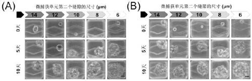
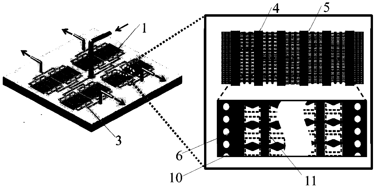
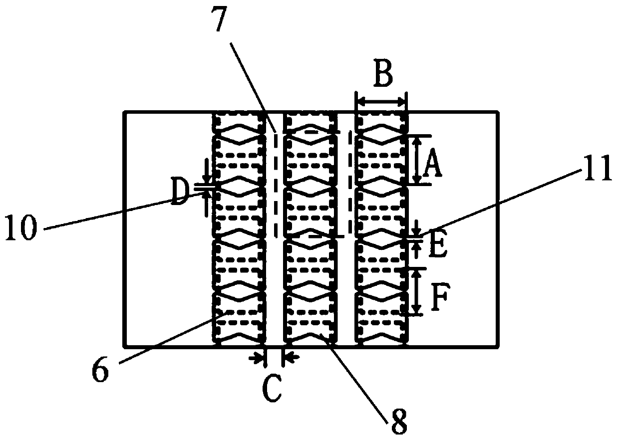
[0064] The applicant's laboratory of the present invention designs the structure and size of the micro-control chip, such as figure 2 As shown, A and B represent the width and length of the microstructure in the single-cell sorting layer, respectively, and the values are 120 μm and 200 μm, respectively, and the width of the constriction in the middle is 90 μm. C represents the distance between the microarrays, and the value is 50 μm, D and E represent the size of the first pore and the second pore between two adjacent microstructures are the same in the capture units of the same column, but their sizes are sequentially reduced by 2 μm in the capture units of different microarrays (ie The size of the first pore in this example is 16 to 8 μm, and the size of the second pore is 14 to 6 μm), such as image 3 As shown, the length of the screening groove formed between two adjacent microstructures is 100 μm, the width of the widest part in the middle is 40 μm, the height L1 of th...
Embodiment 2
[0079] The applicant's laboratory of the present invention designs the structure and size of the micro-control chip, such as figure 2 As shown, A and B represent the width and length of the microstructure in the single-cell sorting layer, respectively, the values are 120 μm and 250 μm, and the width of the constriction in the middle is 90 μm, C represents the distance between the microarrays, the value is 50 μm, D and E represent the size of the first pore and the second pore between two adjacent microstructures are the same in the capture units of the same column, but their sizes are sequentially reduced by 2 μm in the capture units of different microarrays (ie The size of the first pore in this example is 16 to 8 μm, and the size of the second pore is 14 to 6 μm), such as image 3 As shown, the length of the screening groove formed between two adjacent microstructures is 120 μm, the width of the widest part in the middle is 50 μm, the height L1 of the screening groove of ...
PUM
| Property | Measurement | Unit |
|---|---|---|
| length | aaaaa | aaaaa |
| length | aaaaa | aaaaa |
| width | aaaaa | aaaaa |
Abstract
Description
Claims
Application Information
 - R&D Engineer
- R&D Manager
- IP Professional
- Industry Leading Data Capabilities
- Powerful AI technology
- Patent DNA Extraction
Browse by: Latest US Patents, China's latest patents, Technical Efficacy Thesaurus, Application Domain, Technology Topic.
© 2024 PatSnap. All rights reserved.Legal|Privacy policy|Modern Slavery Act Transparency Statement|Sitemap