

Special low-delay intelligent wall switch
A low-latency, switching technology, applied in signal transmission systems, instruments, and adjusting electrical variables, etc., can solve the problems of difficult wireless control and high switching delay, and achieve the effect of improving anti-interference performance, relatively small delay, and avoiding mutual interference
- Summary
- Abstract
- Description
- Claims
- Application Information
AI Technical Summary
Problems solved by technology
Method used
Image

Examples
Embodiment 1
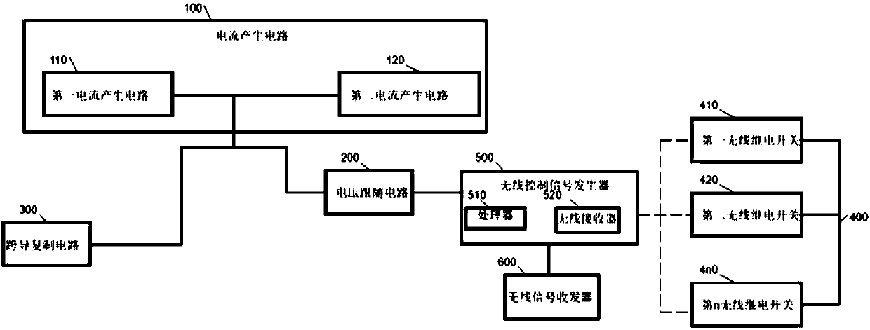
[0045] This embodiment combines Figure 1-Figure 2 The technical scheme of the present invention is described in detail:
[0046] A low-latency smart wall-specific switch that includes:
[0047] The first current generation circuit 110: outputs a first voltage;
[0048] The second current generating circuit 120: outputs a second voltage asynchronous to the first voltage;
[0049] Transconductance replication circuit 300: receiving asynchronous first voltage and second voltage and generating periodic transconductance voltage;
[0050] Wireless signal transceiver 600: receiving a wireless control signal sent by a remote device;
[0051] Wireless control signal generator 500: receiving the transconductance voltage output by the transconductance replica circuit 300 and receiving the wireless control signal output by the wireless signal transceiver 600, and outputting the control voltage under the control of the wireless control signal;
[0052] The relay switch 400: receives the...
Embodiment 2
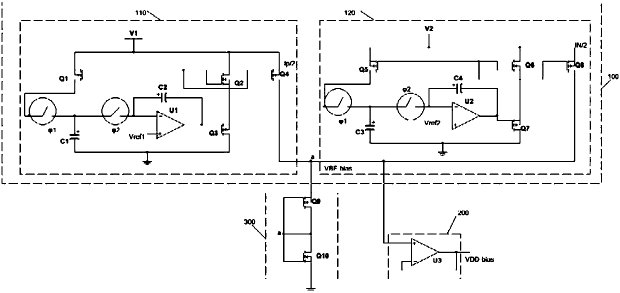
[0074] In the first embodiment, wherein the sixth field effect transistor Q4 and the eighth field effect transistor Q8 belong to the integrated type field effect transistor, this implementation elaborates on the specific circuits of the first current generating circuit 110 and the second current generating circuit 120:
[0075] The first current generation circuit 110 reference image 3 , the first current generation circuit 110 is described in detail below:
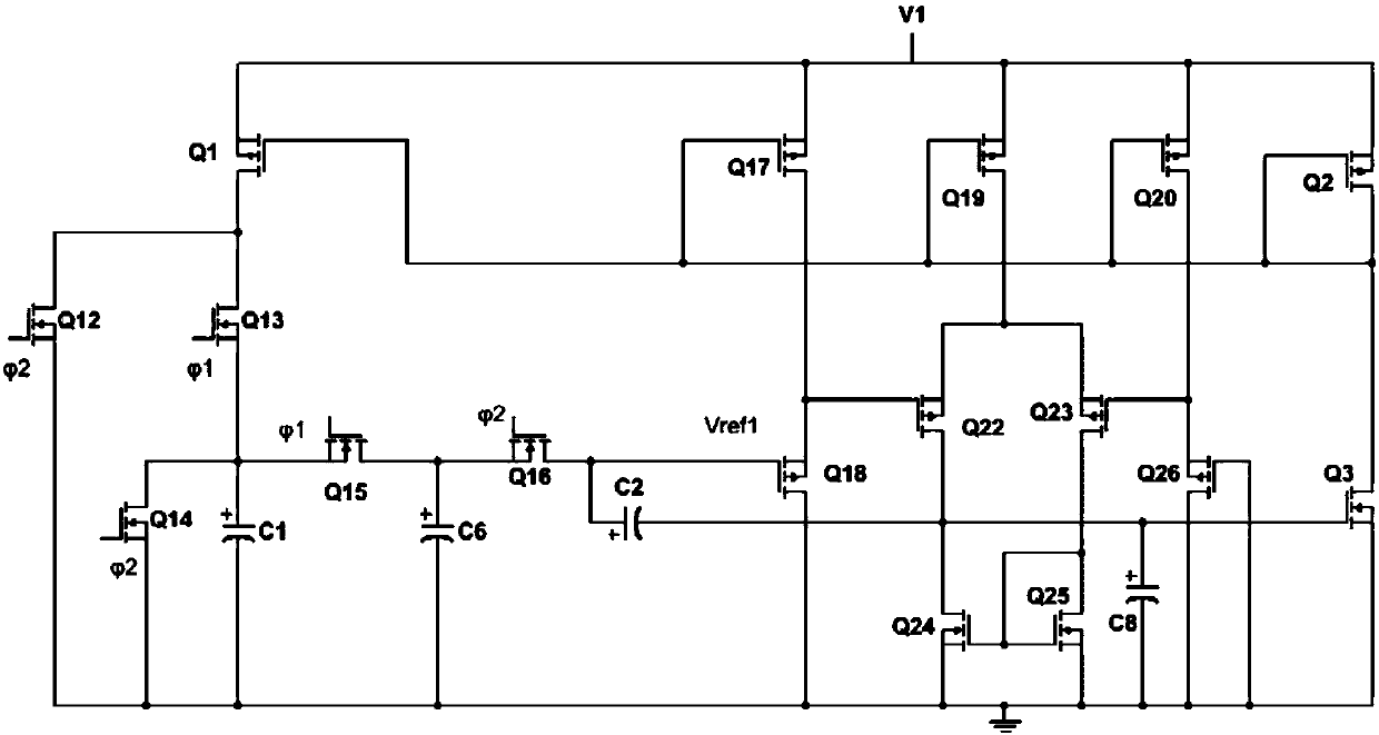
[0076] The third field effect transistor Q1 is a P tube, the source of the third field effect transistor Q1 is connected to the first power supply V1, the drain of the third field effect transistor Q1 is connected to the drain of the eleventh field effect transistor Q12 and the twelfth field effect transistor Q12 The drain of the field effect transistor Q13 is connected, the gate of the eleventh field effect transistor Q12 is connected to the second switch A2, the gate of the twelfth field effect transistor Q13 is connec...
Embodiment 3
[0103] On the basis of the second embodiment, a voltage follower circuit 200 is also provided, the voltage follower circuit 200 receives the transconductance voltage and outputs a standard voltage in isolation;
[0104] The voltage follower circuit 200 includes a third operational amplifier U3, the non-inverting input terminal of the third operational amplifier U3 and the transconductance replica circuit 300 are connected to the first potential point a, the inverting input terminal of the third operational amplifier U3 is connected to the third operational amplifier U3 The output terminal of the third operational amplifier U3 outputs a standard voltage;
[0105] The function of the voltage follower circuit 200 is like an isolator, so that the voltage generating circuit of the present invention and the external circuit will not interfere with each other and affect each other;
[0106] The circuit principle and working conditions of the embodiment are described in detail below: ...
PUM
 Abstract
Description
Claims
Application Information