Fault tolerant architecture of TSV oriented to three-dimensional integrated circuit

An integrated circuit, three-dimensional technology, applied in the direction of circuit, CAD circuit design, electrical components, etc., can solve the problem of poor tolerance of cluster faults, and achieve the effects of avoiding too large differences in length, reducing overhead, and high repair rate

Active Publication Date: 2019-10-11
ANHUI UNIVERSITY OF TECHNOLOGY AND SCIENCE
View PDF6 Cites 4 Cited by
  • Summary
  • Abstract
  • Description
  • Claims
  • Application Information

AI Technical Summary

Problems solved by technology

In response to this problem, Tingting Hwang et al. proposed a ring redundancy architecture, such as figure 1 As shown, although the area overhead is small, the tolerance to cluster faults is relatively poor, and the fault tolerance rate to 2*2 four faults is only about 50%.

Method used


Image

  • Fault tolerant architecture of TSV oriented to three-dimensional integrated circuit
  • Fault tolerant architecture of TSV oriented to three-dimensional integrated circuit
  • Fault tolerant architecture of TSV oriented to three-dimensional integrated circuit

Examples


Embodiment Construction

[0027] In order to make the object, technical solution and advantages of the present invention clearer, the present invention will be further described in detail below in conjunction with the accompanying drawings and embodiments. It should be understood that the specific embodiments described here are only used to explain the present invention, not to limit the present invention.

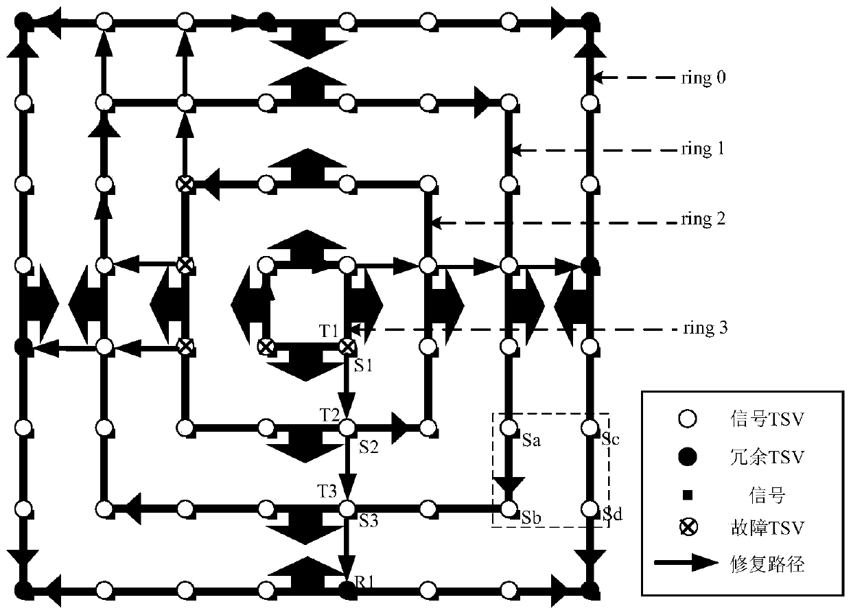
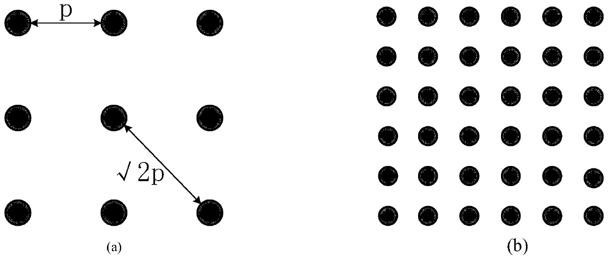
[0028] An important issue in the design process of a three-dimensional integrated circuit is the placement of TSVs, which are mainly responsible for signal transmission between layers. figure 2 (a) is a common 3×3 grid topology, 3 TSVs are placed in the rows and columns of the TSV array, and it is composed of 9 TSVs in total. figure 2 In (a), p is the pitch, that is, the distance between adjacent TSVs. In the grid topology, the TSV distance from the adjacent horizontal and vertical directions is p, and the TSV distance from the center point TSV to the diagonal position is The distance between ...


PUM


Abstract

The invention is suitable for the technical field of the semiconductor, and provides fault tolerant architecture of TSV oriented to three-dimensional integrated circuit. The redundant structure is composed of N layers of annular structures, and N layers of annular structures are equally divided into six regions through six rays; three RTSVs are arranged on each layer of the annular structure, three RTSVs are uniformly distributed on six rays, the RTSVs at the adjacent layers are dislocated and distributed, the RTSV is arranged at the center of the innermost layer of hexagon; the TSVs are arranged by utilizing the specific symmetry and flexibility of the hexagon, and the location for placing the RTSV can be reasonably selected; the redundant structure is divided into multiple uniform regions, and the redundancy rate of each region is improved, thereby guaranteeing the high repair rate of the whole structure; the RTSVs are uniformly distributed in the TSV array, the symmetry of the routing direction is combined, the condition that the repair path length of the fault TSV is large in difference or the time sequence overhead can be avoided, and the overhead is reduced.

Description

technical field [0001] The invention belongs to the technical field of semiconductors and provides a fault-tolerant architecture for TSVs in three-dimensional integrated circuits. Background technique [0002] As the semiconductor process continues to approach the scale of 5nm, 3nm, and 1nm, Moore's Law is also approaching the physical limit. Rico Wiedenbruch, senior vice president of Merck's Global Integrated Circuit Materials Division, said that changing the structure of semiconductor chips through 3D chip structures is the best way to solve the increasingly difficult problem of shrinking process sizes when Moore's Law approaches the physical limit. answer. Three-dimensional integrated circuit (3D IC) uses through-silicon vias (Though Silicon Via, TSV) to connect different layers of devices such as different chips or circuit modules in the vertical direction. Compared with two-dimensional integrated circuits, 3D ICs can effectively reduce the length of interconnection li...

Claims


Application Information

Patent Timeline
Patent Type & Authority Applications(China)
IPC IPC(8): H01L27/02H01L23/48G06F17/50
CPCH01L27/0207H01L23/481G06F30/398G06F2115/06
Inventor 倪天明束月鲁麟代广珍韩名君高文根瞿成明朱世东
Owner ANHUI UNIVERSITY OF TECHNOLOGY AND SCIENCE
Why Eureka
Try Eureka