Active pixel swing extension system and method for CMOS image sensor

A technology of an image sensor and an expansion method, applied in the field of semiconductor integrated circuits, can solve problems such as swing attenuation, and achieve the effects of swing enhancement, output swing enhancement, wide range of high dynamics and high sensitivity

Active Publication Date: 2019-10-15
XIAN UNIV OF TECH
View PDF5 Cites 3 Cited by
  • Summary
  • Abstract
  • Description
  • Claims
  • Application Information

AI Technical Summary

Problems solved by technology

[0004] The purpose of the present invention is to provide an active pixel swing expansion method for CMOS image sensors, which solves the problem of swing attenuation in the readout process of the CMOS image sensor 8T structure that exists in the prior art

Method used


Image

  • Active pixel swing extension system and method for CMOS image sensor
  • Active pixel swing extension system and method for CMOS image sensor
  • Active pixel swing extension system and method for CMOS image sensor

Examples


Embodiment Construction

[0022] The present invention will be described in detail below in conjunction with the accompanying drawings and specific embodiments.

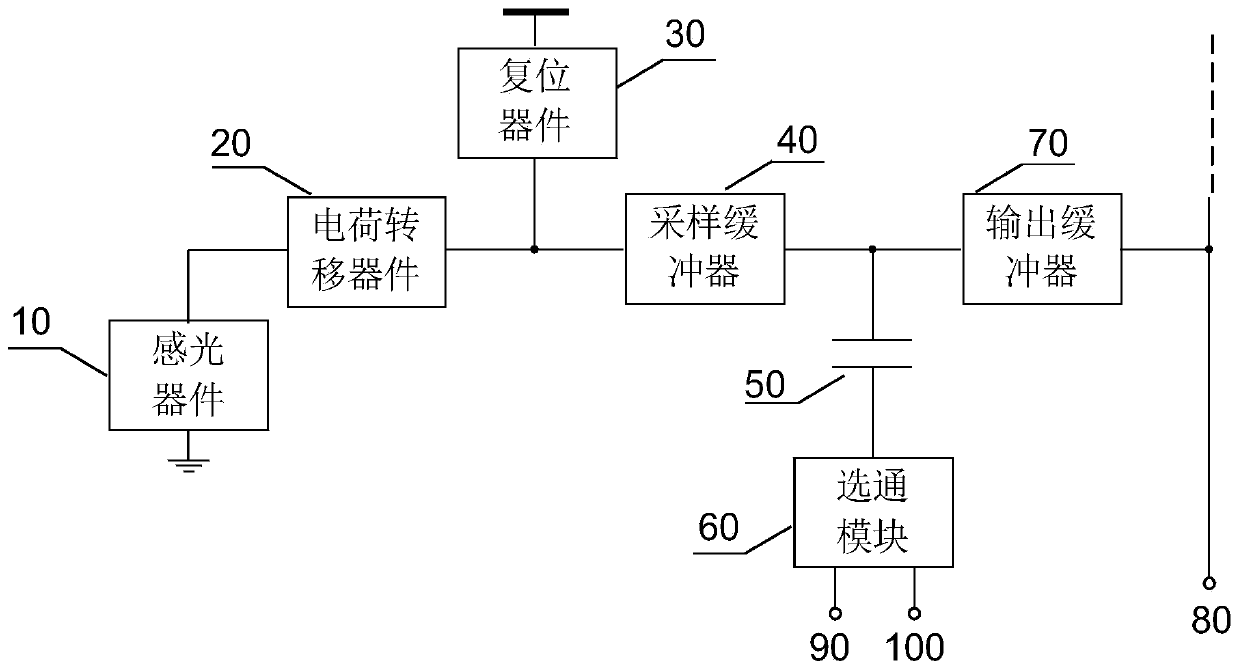
[0023] The active pixel swing expansion system for a CMOS image sensor includes a photosensitive device 10, one end of the photosensitive device 10 is grounded, and the other end is sequentially connected with a charge transfer device 20 and a reset device 30 for realizing the reset of the photosensitive device 10, The common end that the charge transfer device 20 is connected with the reset device 30 is connected with the input end of the sampling buffer 40, the output end of the sampling buffer 40 realizes the function of keeping through the energy storage element 50, and the other end of the energy storage element 50 is connected with the gating module 60, the two input ends of the gating module 60 are external signal A90 and external signal B100 respectively, the output end of the gating module 60 is connected to the inside of the pixel un...


PUM


Abstract

The invention discloses an active pixel swing extension method for a CMOS image sensor. The problem that the swing amplitude of the active pixel unit is limited due to threshold loss and other reasonsin the electric signal output process is solved. The method is characterized in that the lower pole plate of the sampling and holding capacitor is connected to a ground level or a low voltage duringsampling of the pixel unit and is connected to a power level or a high voltage during output of the pixel unit through a method of switching the lower pole plate of the sampling and holding capacitorby a switch, so that the swing amplitude of photoelectric signals on a column line is increased. In order to ensure the influence of the method on the filling factor of the pixel unit, switch switching and high and low voltage are realized outside an active pixel unit area array. The invention provides a programmable bootstrap swing lifting mechanism based on area array external voltage, providesa solution for a large-area-array large-full-well active pixel CMOS image sensor, guarantees the complete response of an active pixel circuit to full-well charges, improves the full-well capability ofthe CMOS image sensor, and enlarges the dynamic range of the CMOS image sensor.

Description

technical field [0001] The invention belongs to the technical field of semiconductor integrated circuits, and specifically relates to an image sensor, array data reading, high-speed and high-precision photoelectric conversion front-end acquisition system, and also relates to an active pixel swing expansion method for a CMOS image sensor. Background technique [0002] In high-speed photography, automation and industrial applications, due to the requirements of shooting fast moving targets, CMOS image sensors with global exposure function are usually used. In low-orbit aerospace applications, because the object moves faster at the focal plane, if the imaging device uses a rolling shutter exposure device, the "motion distortion" of the image will occur. Similarly, in high-orbit applications, "motion distortion" can occur due to platform stability issues. Therefore, the current aerospace models have a strong demand for global exposure CMOS image sensor devices. It can be seen ...

Claims


Application Information

Patent Timeline
Patent Type & Authority Applications(China)
IPC IPC(8): H04N5/374H04N5/3745
CPCH04N25/76H04N25/77
Inventor 郭仲杰余宁梅
Owner XIAN UNIV OF TECH
Why Eureka
Try Eureka