Semiconductor processing device with cleaning function and cleaning method of semiconductor processing device using the same

A process equipment and semiconductor technology, applied in cleaning methods and appliances, semiconductor/solid-state device manufacturing, cleaning hollow objects, etc., can solve problems such as inhalation of harmful substances by workers, corrosion of pump parts, failure of semiconductor process equipment, etc., to achieve a solution Reduced performance or frequent malfunctions, effects of preventing contamination

Active Publication Date: 2019-11-01
GIGALANE CO LTD
View PDF4 Cites 2 Cited by
  • Summary
  • Abstract
  • Description
  • Claims
  • Application Information

AI Technical Summary

Problems solved by technology

However, the problem with this cleaning process is that workers may inhale harmful substances
However, this method has a problem in that the fume is fixed in the form of powder in the pumping pipe connecting the chamber and the pump, which has a temperature relatively lower than the temperature inside the chamber, so that the performance of the semiconductor process equipment is reduced.
Also, there is a problem that when a pump is used, since chlorine is discharged faster than hydrogen chloride is produced, chlorine is directly sucked into the pump, causing corrosion to parts of the pump, and semiconductor process equipment malfunctions

Method used


Image

  • Semiconductor processing device with cleaning function and cleaning method of semiconductor processing device using the same
  • Semiconductor processing device with cleaning function and cleaning method of semiconductor processing device using the same
  • Semiconductor processing device with cleaning function and cleaning method of semiconductor processing device using the same

Examples


Embodiment Construction

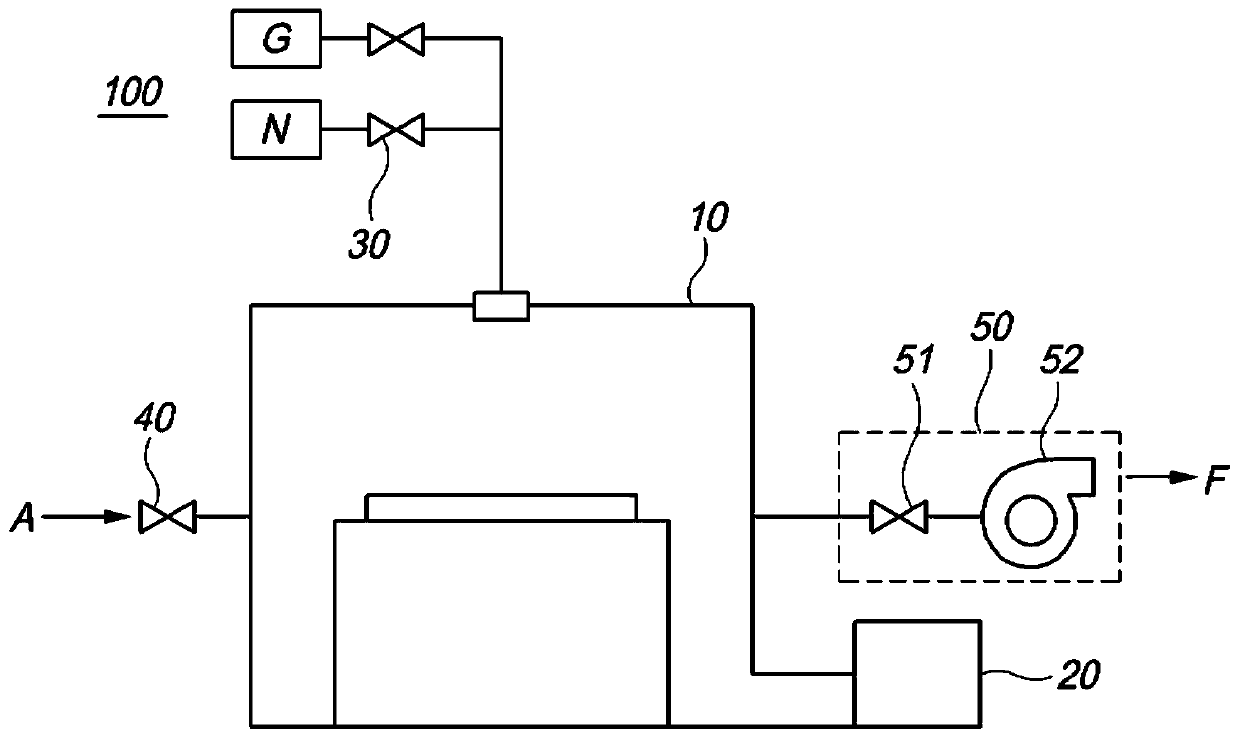
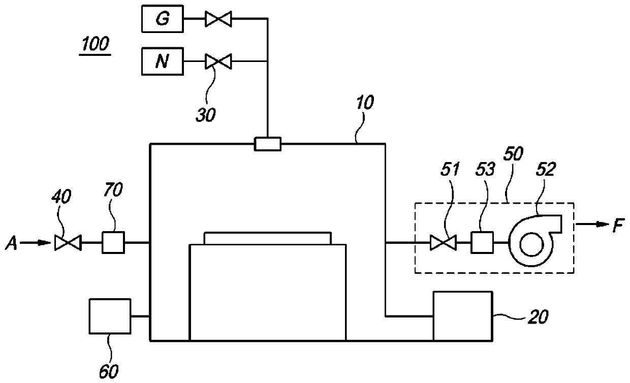
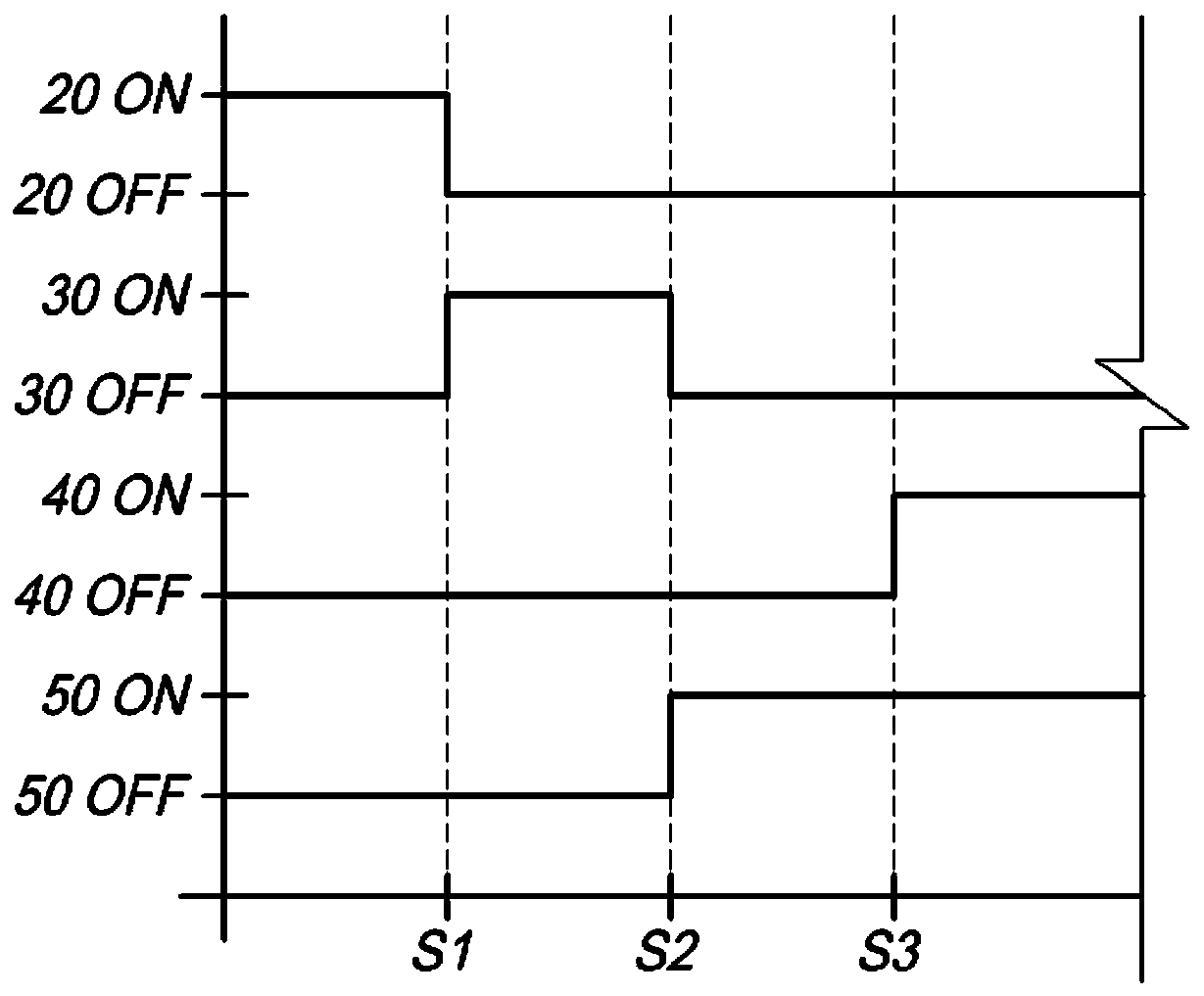
[0041] Hereinafter, with reference to the accompanying drawings, the semiconductor process equipment with cleaning function and the cleaning method of the semiconductor process equipment utilizing the cleaning function according to the present invention will be described in detail.

[0042] Generally, in order to etch a thin film formed on a substrate, chlorine (Cl)-based (Cl 2 / Ar, Cl 2 / N 2 , Cl 2 / He, Cl 2 / BCl 3 / Ar, BCl 3 / Ar, BrCl 3 、SiCl 4 / Ar, CCl 2 f 2 / H 2 / Ar, etc.) gas is used as the process gas. When the etching process is repeatedly performed using such a process gas, reaction by-products are generated inside the chamber. The reaction by-products are deposited inside the chamber and act as a source of contamination to the substrate in subsequent processes, so in order to remove them, the chamber needs to be cleaned periodically. As a method of cleaning the chamber, there is a method in which a worker opens the chamber lid to clean the inside of the ch...


PUM


Abstract

The present invention relates to a cleaning method of a semiconductor process device, including: a chamber providing a substrate processing space therein; a first gas exhaust unit exhausting process gas from the inside of the chamber; a first gas supply unit supplying inert gas into the chamber; a second gas supply unit supplying cleaning gas into the chamber and generating fume in the chamber; and a second gas exhaust unit exhausting the inert gas, the cleaning gas, the fume and mixed gas thereof from the inside of the chamber, wherein the second gas exhaust unit includes an inhalation fan controlling the displacement of the inert gas, the cleaning gas, the fume and the mixed gas thereof.

Description

technical field [0001] The invention relates to semiconductor process equipment with cleaning function and a cleaning method for semiconductor process equipment utilizing the cleaning function. Background technique [0002] Semiconductor process equipment is a device that mounts a substrate on a chuck and processes the substrate through a semiconductor process. [0003] For example, an apparatus for processing a substrate by a semiconductor process may inject process gas into a chamber to perform one or more of plasma evaporation and etching. Generally, in order to etch a thin film formed on a substrate, a chlorine (Cl)-based gas is used as a process gas. [0004] When such a chlorine-based gas is used as a process gas and an etching process is repeatedly performed, reaction by-products are generated inside the chamber. The generated reaction by-products are deposited inside the chamber and act as a contamination source to the substrate in subsequent processes, thus requir...

Claims


Application Information

Patent Timeline
Patent Type & Authority Applications(China)
IPC IPC(8): H01J37/32B08B9/093
CPCB08B9/093H01J37/32862H01L21/02046H01L21/67028H01L21/67098H01L21/67242
Inventor 金亨源郑明教郑熙锡
Owner GIGALANE CO LTD
Why Eureka
Try Eureka