Integrated circuit, film removing method of integrated circuit and film removal arranging device of integrated circuit

A technology of integrated circuits and equipment, applied in the field of integrated circuit tear-off typesetting equipment, can solve the problems that integrated circuits cannot be collected, chips are not collected, and cannot be processed continuously, so as to achieve smooth film peeling, avoid disorder and structure. simple effect

Inactive Publication Date: 2019-11-08
NINGBO YINZHOU TEERFEI ELECTRONICS CO LTD
View PDF6 Cites 18 Cited by
  • Summary
  • Abstract
  • Description
  • Claims
  • Application Information

AI Technical Summary

Problems solved by technology

This patent can only separate one chip at a time, which is inefficient, and the chips taken out are not collected
[0004] To sum up, the existing integrated circuit film tearing operation has the problems of low automation of loading and unloading, continuous processing, cumbersome glue tearing process, and inability to complete the collection of integrated circuits

Method used


Image

  • Integrated circuit, film removing method of integrated circuit and film removal arranging device of integrated circuit
  • Integrated circuit, film removing method of integrated circuit and film removal arranging device of integrated circuit
  • Integrated circuit, film removing method of integrated circuit and film removal arranging device of integrated circuit

Examples


Embodiment Construction

[0032] The following will clearly and completely describe the technical solutions in the embodiments of the present invention with reference to the accompanying drawings in the embodiments of the present invention. Obviously, the described embodiments are only some, not all, embodiments of the present invention.

[0033] In describing the present invention, it should be understood that the terms "upper", "lower", "front", "rear", "left", "right", "top", "bottom", "inner", " The orientation or positional relationship indicated by "outside" and other indications are based on the orientation or positional relationship in the drawings, and are only for the convenience of describing the present invention and simplifying the description, rather than indicating or implying that the device or element referred to must have a specific orientation, use a specific orientation construction and operation, therefore, should not be construed as limiting the invention.

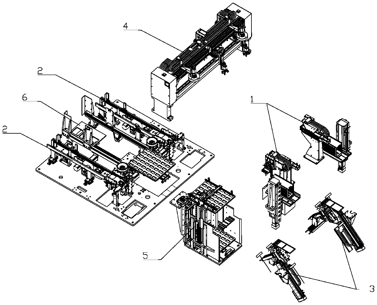
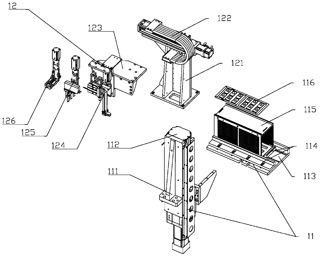
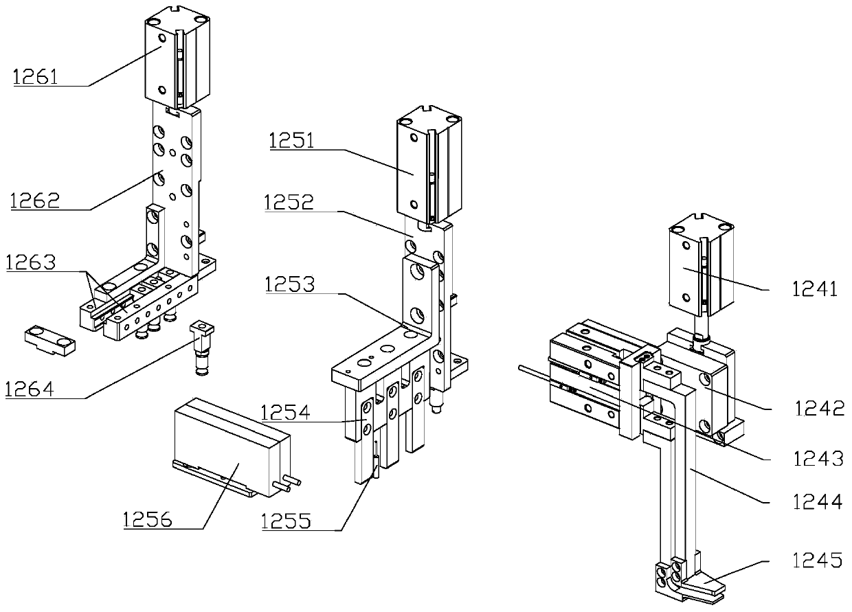
[0034] like figure 1 ...


PUM


Abstract

The invention relates to the technical field of integrated circuit manufacturing, and discloses a film removal arranging device of an integrated circuit. The film removal arranging device comprises aframe, two symmetrically arranged carrier plate feeding devices, two symmetrically arranged carrier plate conveying line devices, two symmetrically arranged film removing devices, a carrying manipulator, a visual detection device, a tray feeding device and a tray conveying line device, wherein the carrier plate feeding devices, the carrier plate conveying line devices, the film removing devices, the carrying manipulator, the visual detection device, the tray feeding device and the tray conveying line device are arranged on the frame; the film removing devices are positioned below the carrier plate feeding devices; the carrier plate conveying line devices are connected with the carrier plate feeding devices; the tray feeding device is positioned between the two carrier plate feeding devices; the tray conveying line device is positioned between the two carrier plate conveying line devices and is connected with the tray feeding device; and the carrying manipulator and the visual detectiondevice are arranged on the frame and are positioned above the carrier plate conveying line devices and the tray conveying line device. The film removal arranging device has the advantages of being efficient and accurate in glue removing, automatic in feeding and discharging, high in processing efficiency and capable of collecting and arranging the integrated circuit.

Description

technical field [0001] The invention relates to the technical field of integrated circuit manufacturing, in particular to an integrated circuit tear film typesetting device and working method. Background technique [0002] With the development of society, semiconductor devices and their packaging are becoming thinner and miniaturized. In some cases, the back of the integrated circuit needs to be protected by a protective film to prevent damage to the integrated circuit chip. When packaging, the protective film should be peeled off. In the existing integrated circuit production process, because the bottom film is bonded to the chip through an adhesive, the existing film tearing equipment cannot effectively reduce the viscosity of the bottom film, resulting in low tearing efficiency and easy damage to the backside of the integrated circuit. metal damage. [0003] The State Intellectual Property Office published the publication number CN207068801U on 2018.03.02, and the paten...

Claims


Application Information

Patent Timeline
Patent Type & Authority Applications(China)
IPC IPC(8): B65B69/00B65G47/91H01L21/67H01L21/683
CPCB65B69/00H01L21/67126H01L21/67242H01L21/67294H01L21/67703H01L21/683
Inventor 曲容容魏星魏芙蓉杨立慈
Owner NINGBO YINZHOU TEERFEI ELECTRONICS CO LTD
Why Eureka
Try Eureka