

Laminate, method for producing same, and method for producing device structure using same
a technology of laminates and methods, applied in can solve the problems of inapplicability to ceramics, limited field of ceramics, and inability to adapt to the field of laminates, and achieve the effects of easy peeling, good adhesion parts, and easy acquisition of device-bearing polyimide films
- Summary
- Abstract
- Description
- Claims
- Application Information
AI Technical Summary
Benefits of technology
Problems solved by technology
Method used
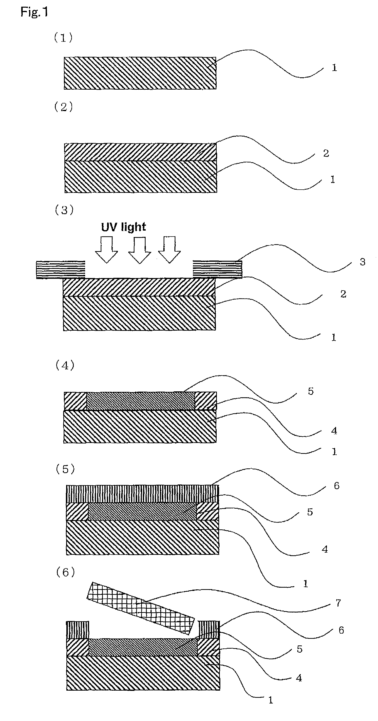
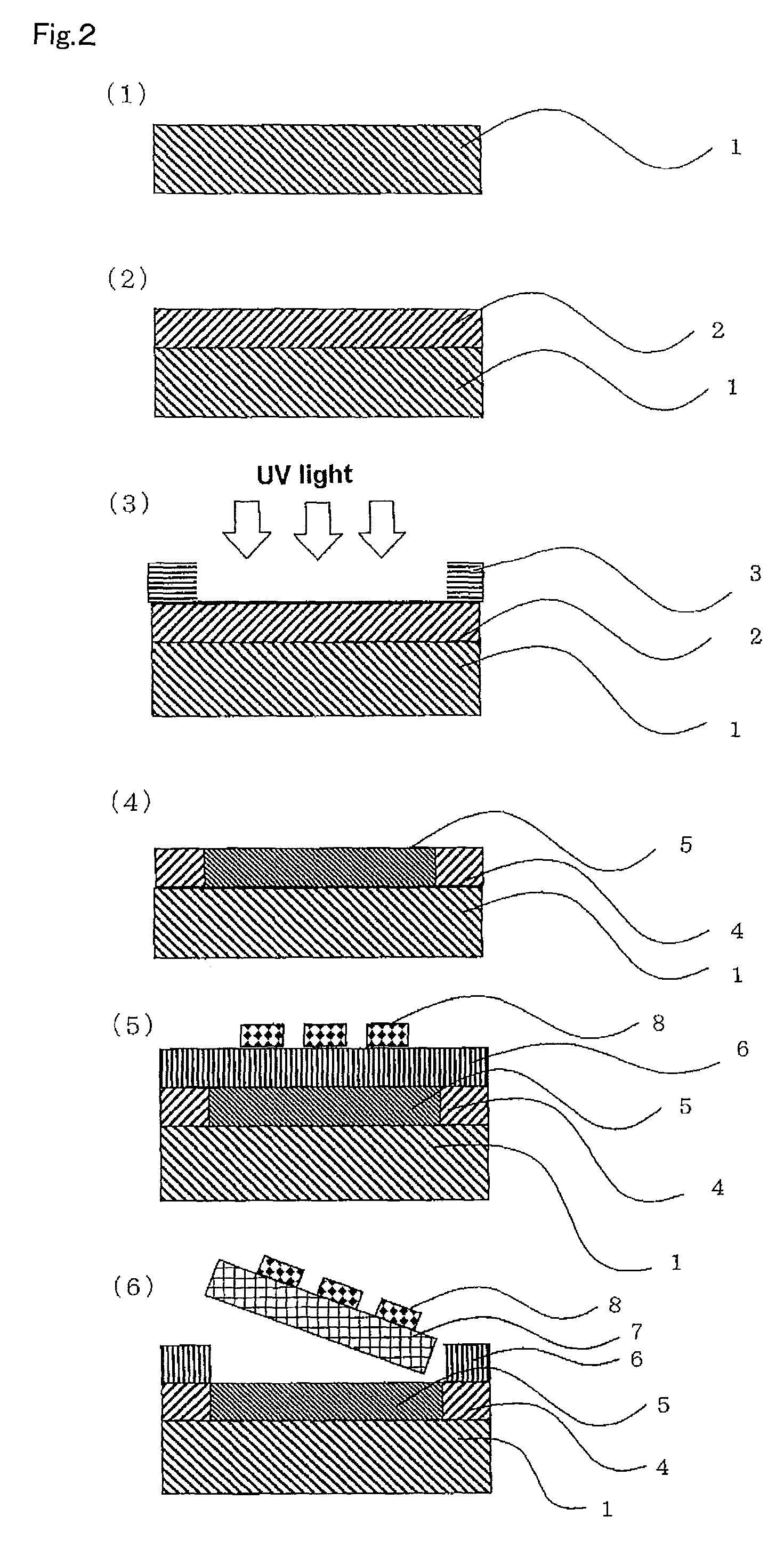
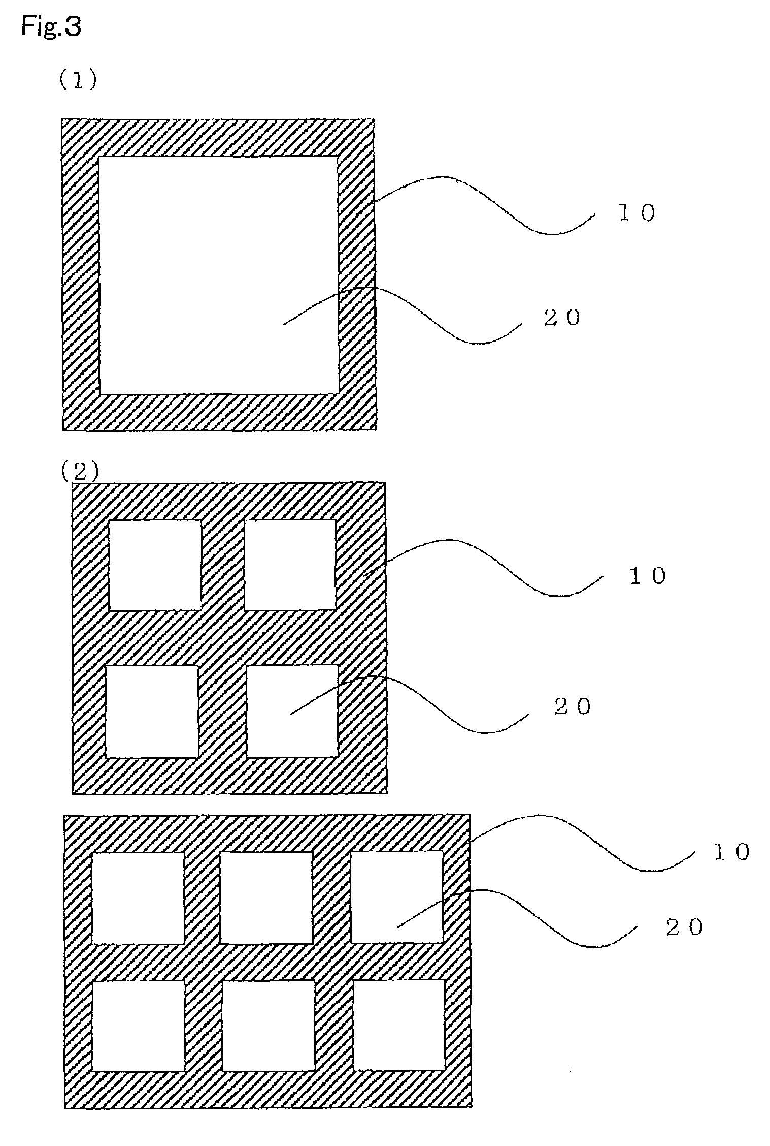
Image

Examples
examples
[0163]Hereinafter, the present invention will be described concretely by way of Examples and Comparative Examples; however, the present invention is not limited to Examples below. The evaluation methods for physical properties in Examples below are as follows.
[0164]The thicknesses of a polyimide film and respective layers (a-layer, b-layer) constituting the polyimide film were measured by using a micrometer (“Millitron 1245D”, manufactured by Feinpruf).
[0165]Strip-like specimens with a size of 100 mm×10 mm in the machine direction (MD direction) and in the transverse direction (TD direction) were cut out from each polyimide film to be measured, and ensile elasticity, tensile strength, and tensile elongation at break of each specimen were measured in the MD direction and in the TD direction, respectively, under conditions of a tension speed of 50 mm / minute and an inter-chuck distance of 40 mm by using a tension testing machine (“Autograph (R); model AG-5000 A”, manufactured by SHIMAD...
production examples 1 and 2
(Preparation of Polyamide Acid Solutions A1 and A2)
[0218]After a reaction container equipped with a nitrogen introduction pipe, a thermometer, and a stirring rod was replaced with nitrogen, 223 parts by mass of 5-amino-2-(p-aminophenyl)benzoxazole and 4416 parts by mass of N,N-dimethylacetamide were added and completely dissolved; and next, 217 parts by mass of pyromellitic acid dianhydride was added thereto in combination with a dispersion obtained by dispersing colloidal silica in dimethylacetamide (“Snowtex (registered trademark) DMAC-ST 30”, manufactured by Nissan Chemical Industries, Ltd.) as a lubricant in an amount such that the addition amount of silica (lubricant) was as shown in Table 1 (mass % to the total weight of the polymer solid matter in the polyamide acid solution), and the mixture was stirred at a reaction temperature of 25° C. for 24 hours to obtain brown and viscous polyamide acid solutions A1 and A2.
[0219]
TABLE 1ProductionProductionUnitExample 1Example 2Polyami...
production examples 3 and 4
(Preparation of Polyamide Acid Solutions B1 and B2)
[0220]After a reaction container equipped with a nitrogen introduction pipe, a thermometer, and a stirring rod was replaced with nitrogen, 545 parts by mass of pyromellitic anhydride and 500 parts by mass of 4,4′-diaminodiphenyl ether were dissolved in 8000 parts by mass of N,N-dimethylacetamide and the resultant was added thereto, and a dispersion obtained by dispersing colloidal silica in dimethylacetamide (“Snowtex (registered trademark) DMAC-ST 30”, manufactured by Nissan Chemical Industries, Ltd.) was added as a lubricant in an amount such that the addition amount of silica (lubricant) was as shown in Table 2 (mass % to the total weight of the polymer solid matter in the polyamide acid solution), and the mixture was stirred while keeping the temperature at 20° C. or lower for 24 hours to obtain polyamide acid solutions B1 and B2.
[0221]
TABLE 2ProductionProductionUnitExample 3Example 4Polyamide acidB1B2solutionLubricant typeSilic...
PUM
| Property | Measurement | Unit |
|---|---|---|
| temperature | aaaaa | aaaaa |
| temperature | aaaaa | aaaaa |
| temperature | aaaaa | aaaaa |
Abstract
Description
Claims
Application Information