Mask-free direct writing photolithography system

A lithography system and maskless technology, applied in the field of micro-nano processing devices, can solve the problems of low processing efficiency and high processing cost, and achieve the effects of improving lithography efficiency, scanning rate and scanning freedom.

Inactive Publication Date: 2019-11-12
SHANGHAI INST OF OPTICS & FINE MECHANICS CHINESE ACAD OF SCI
View PDF9 Cites 3 Cited by
  • Summary
  • Abstract
  • Description
  • Claims
  • Application Information

AI Technical Summary

Problems solved by technology

The above-mentioned laser direct writing system can only perform single-beam direct writing, so the processing efficiency is low and the processing cost is high

Method used


Image

  • Mask-free direct writing photolithography system
  • Mask-free direct writing photolithography system
  • Mask-free direct writing photolithography system

Examples


Embodiment Construction

[0021] The present invention will be further described below in conjunction with the accompanying drawings and implementation examples, but the protection scope of the present invention should not be limited thereby.

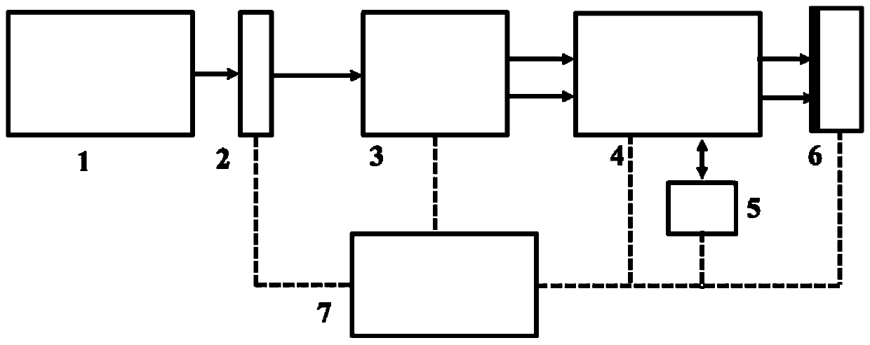
[0022] see first figure 1 , figure 1 It is a schematic diagram of the composition of the maskless direct writing lithography system of the present invention. It can be seen from the figure that the maskless direct writing lithography system of the present invention includes a direct writing light source 1, an energy control unit 2, a laser beam splitting control and scanning unit 3, Focus servo unit 4, red light detection unit 5, multi-axis workpiece platform 6 and control unit 7, along the direction of the output light of the direct writing light source 1 are the energy control unit 2, laser beam splitting control and scanning in sequence Unit 3, focus servo unit 4, red light detection unit 5 and multi-axis workpiece platform 6, the control unit 7 is respectiv...


PUM


Abstract

The invention discloses a mask-free direct writing photolithography system; the mask-free direct writing photolithography system comprises a direct writing light source, an energy control unit, a laser beam splitting control and scanning unit, a focusing servo unit, a red light detection unit, a multi-axis workpiece platform and a control unit. Under the overall control of the control unit, the light emitted by the direct writing light source irradiates onto the laser beam splitting control and scanning unit through the control of the energy control unit; after being controlled by the laser beam splitting control and scanning unit, the light is focused by the focusing servo unit and detected by the red light detection unit; and finally the multiple paths of light beams are focused on photoresist in parallel for direct writing. According to the photolithography system, independent control of multiple light beams, parallel direct writing and two-dimensional galvanometer scanning can be realized, and the photolithography efficiency is improved in a multiplied mode compared with a single-point scanning system. The scanning speed and the scanning freedom degree of a direct writing photolithography machine are improved.

Description

technical field [0001] The invention relates to a micro-nano processing device, in particular to a maskless direct writing photolithography system. [0002] technical background [0003] In recent years, with the rapid development of the integrated circuit industry, the emergence of smart devices such as smartphones and smart TVs has led to a blowout development trend in the semiconductor industry. In the past few decades, the minimum line width of the photolithography process has been reduced at a rate of 30% every 3 years. The feature size of semiconductor devices has reached 7nm from 32nm, 22nm, and 16nm. With the reduction of the minimum feature size, the number of transistors per unit area continues to increase, and the computing speed of the chip is continuously improved. As one of the key technologies in chip manufacturing, photolithography plays a decisive role in the minimum feature size of the chip. Therefore, The development of photolithography technology restric...

Claims


Application Information

Patent Timeline
Patent Type & Authority Applications(China)
IPC IPC(8): G03F7/20
CPCG03F7/704
Inventor 胡敬佩张冲朱玲琳曾爱军黄惠杰
Owner SHANGHAI INST OF OPTICS & FINE MECHANICS CHINESE ACAD OF SCI
Why Eureka
Try Eureka